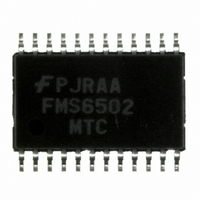
FMS6502MTC24 Fairchild Semiconductor, FMS6502MTC24 Datasheet - Page 9

FMS6502MTC24
Manufacturer Part Number
FMS6502MTC24
Description
IC VIDEO SWITCH 8IN/6OUT 24TSSOP
Manufacturer
Fairchild Semiconductor
Datasheet
1.FMS6502MTC24X.pdf
(13 pages)
Specifications of FMS6502MTC24
Function
Video Crosspoint Switch
Circuit
1 x 8:6
Current - Supply
55mA
Operating Temperature
-40°C ~ 85°C
Mounting Type
Surface Mount
Package / Case
24-TSSOP
Lead Free Status / RoHS Status
Lead free / RoHS Compliant
Available stocks
Company
Part Number
Manufacturer
Quantity
Price
Company:
Part Number:
FMS6502MTC24X
Manufacturer:
Fairchild Semiconductor
Quantity:
31 989
Part Number:
FMS6502MTC24X
Manufacturer:
FAIRCHILD/仙童
Quantity:
20 000
© 2006 Fairchild Semiconductor Corporation
FMS6502 Rev. 1.0.0
Applications Information
Input Clamp / Bias Circuitry
The FMS6502 can accommodate AC- or DC-coupled
inputs. Internal clamping and bias circuitry are provided
to support AC-coupled inputs. These are selectable
through the CLMP bits via the I
For DC-coupled inputs, the device should be pro-
grammed to use the 'bias' input configuration. In this con-
figuration, the input is internally biased to 625mV through
a 100kΩ resistor. Distortion is optimized with the output
levels set between 250mV above ground and 500mV
below the power supply.
With AC-coupled inputs, the FMS6502 uses a simple
clamp rather than a full DC-restore circuit. For video sig-
nals with and without sync; (Y,CV,R,G,B), the lowest volt-
age at the output pins is clamped to approximately
300mV above ground.
If symmetric AC-coupled input signals are used
(Chroma,Pb,Pr,Cb,Cr), the bias circuit can be used to
center them within the input common range. The aver-
age DC value at the output is approximately 1.27V.
Figure 8 shows the clamp mode input circuit and the
internally controlled voltage at the input pin for AC-cou-
pled inputs.
Figure 9 shows the bias mode input circuit and the inter-
nally controlled voltage at the input pin for AC-coupled
inputs.
Video source must
be AC coupled
Video source must
be AC coupled
Figure 8. Clamp Mode Input Circuit
Figure 9. Bias Mode Input Circuit
75
Lowest voltage
Average voltage
set to 125mV
set to 625mV
0.1µF
0.1µF
75
2
C-compatible interface.
FMS6502
Clamp
Input
FMS6502
Input
Bias
9
Output Configuration
The FMS6502 outputs may be AC or DC-coupled. DC-
coupled loads can drive a 150Ω load. AC-coupled out-
puts are capable of driving a single, doubly terminated
video load of 150Ω. An external transistor is needed to
drive DC low-impedance loads.
should be connected as indicated in Figure 10.
Configure AC-coupled loads as shown in Figure 11.
When an output channel is not connected to an input, the
input to that particular channel’s amplifier is forced to
approximately 150mV. The output amplifier is still active
unless specifically disabled by the I
output levels depend on the programmed gain for that
channel.
Driving Capacitive Loads
When driving capacitive loads, use a 10Ω-series resis-
tance to buffer the output, as indicated in Figure 12.
Figure 10. DC-Coupled Load Connection
Figure 11. AC-Coupled Load Connection
Figure 12. Driving Capacitive Loads
FMS6502
Amplifier
FMS6502
Output
Amplifier
FMS6502
Amplifier
Output
Output
75
10
75
220µF
2
DC-coupled outputs
C interface. Voltage
75
75
www.fairchildsemi.com


