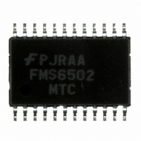
FMS6502MTC24 Fairchild Semiconductor, FMS6502MTC24 Datasheet - Page 8

FMS6502MTC24
Manufacturer Part Number
FMS6502MTC24
Description
IC VIDEO SWITCH 8IN/6OUT 24TSSOP
Manufacturer
Fairchild Semiconductor
Datasheet
1.FMS6502MTC24X.pdf
(13 pages)
Specifications of FMS6502MTC24
Function
Video Crosspoint Switch
Circuit
1 x 8:6
Current - Supply
55mA
Operating Temperature
-40°C ~ 85°C
Mounting Type
Surface Mount
Package / Case
24-TSSOP
Lead Free Status / RoHS Status
Lead free / RoHS Compliant
Available stocks
Company
Part Number
Manufacturer
Quantity
Price
Company:
Part Number:
FMS6502MTC24X
Manufacturer:
Fairchild Semiconductor
Quantity:
31 989
Part Number:
FMS6502MTC24X
Manufacturer:
FAIRCHILD/仙童
Quantity:
20 000
© 2006 Fairchild Semiconductor Corporation
FMS6502 Rev. 1.0.0
Acknowledge
The number of data bytes transferred between the start
and stop conditions from transmitter to receiver is unlim-
ited. Each byte of eight bits is followed by an acknowl-
edge bit. The acknowledge bit is a HIGH level signal put
on the bus by the transmitter while the master generates
an extra acknowledge-related clock pulse. The slave
receiver addressed must generate an acknowledge after
the reception of each byte. A master receiver must gen-
erate an acknowledge after the reception of each byte
clocked out of the slave transmitter.
I
Before any data is transmitted on the I
which is to respond is addressed first. The addressing is
always carried out with the first byte transmitted after the
3.3V Operation
The FMS6502 operates from a single 3.3V supply. With
V
digital input high (V
2
cc
C Bus Protocol
= 3.3V, the digital input low (V
SCL FROM
MASTER
DATA OUTPUT
BY TRANSMITTER
DATA OUTPUT
BY RECEIVER
Figure 7. Write Register Address to Pointer Register; Write Data to Selected Register
START BY
MASTER
ih
SCL
SDA
) is 1.8V to 2.9V.
START
condition
A6
1
A5
SERIAL BUS ADDRESS BYTE
il
Figure 6.
) is 0V to 1V and the
A4
2
FRAME1
C bus, the device
A3
1
SCL(CONTINUED)
SDA(CONTINUED)
A2
Acknowledgement on the I
A1
A0
R/W
ACK. BY
FMS6502
2
D7
8
9
1
The device that acknowledges must pull down the SDA
line during the acknowledge clock pulse so the SDA line
is stable LOW during the HIGH period of the acknowl-
edge-related clock pulse (set-up and hold times must be
taken into consideration). A master receiver must signal
an end of data to the transmitter by not generating an
acknowledge on the last byte clocked out of the slave. In
this event, the transmitter must leave the data line HIGH
to enable the master to generate a stop condition.
start procedure. The I
write to the FMS6502 is shown in Figure 7.
D7
D6
1
D6
D5
ADDRESS POINTER REGISTER BYTE
D5
D4
DATA BYTE
FRAME 3
D4
D3
2
FRAME 2
C Bus
D3
D2
8
D2
D1
D1
D0
2
C bus configuration for a data
ACK. BY
FMS6502
D0
9
ACK. BY
FMS6502
clock pulse for
acknowledgement
9
STOP BY
MASTER
9
www.fairchildsemi.com


