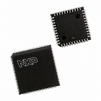
SCC68681E1A44,512 NXP Semiconductors, SCC68681E1A44,512 Datasheet - Page 18

SCC68681E1A44,512
Manufacturer Part Number
SCC68681E1A44,512
Description
IC DUART 44PLCC
Manufacturer
NXP Semiconductors
Datasheet
1.SCC68681C1A44512.pdf
(29 pages)
Specifications of SCC68681E1A44,512
Features
False-start Bit Detection
Number Of Channels
2, DUART
Fifo's
3Bit
Voltage - Supply
5V
With Auto Flow Control
Yes
With False Start Bit Detection
Yes
With Cmos
Yes
Mounting Type
Surface Mount
Package / Case
44-LCC (J-Lead)
Lead Free Status / RoHS Status
Lead free / RoHS Compliant
Other names
935274496512
SCC68681E1A44
SCC68681E1A44
SCC68681E1A44
SCC68681E1A44
Available stocks
Company
Part Number
Manufacturer
Quantity
Price
Company:
Part Number:
SCC68681E1A44,512
Manufacturer:
NXP Semiconductors
Quantity:
10 000
Philips Semiconductors
Output Port Notes
The output ports are controlled from three places: the OPCR
register, the OPR register, and the MR registers. The default source
of data for the OP[7:0] pins is the OPR register. When the OPR is
the source for the OP pins, the pins will drive the complement
(inverse) of data in the OPR register.
The OPCR register, the MR register, and the Command register
control the data source for the OP pins. It is this ‘multi-source’
feature of the OP pins that allows them to give the 485 turn-around,
RTS, DMA, interrupt, and various other internal clock signals.
The OPCR controls the source of the data for the output ports OP2
through OP7. The data source for output ports OP0 and OP1 is
controlled by the MR and CR registers. When the OPR is the source
of the data for the output ports, the data at the ports is inverted from
that in the OPR register.
The content of the OPR register is controlled by the ‘Set and Reset
Output Port Bits Commands’. These commands are actually the
addresses at 0xE and 0xF, respectively. When these commands are
used, action takes place only at the bit locations where ones exist
on the data bus. For example, a one in bit location 5 of the data
word used with the ‘Set Output Port Bits’ command will result in
OPR[5] being set to one. The OP[5] pin would then drive a logical
zero (V
associated with the ‘Reset Output Ports Bits’ command would set
OPR[5] to zero, and hence, the pin OP[5] will drive to a one (V
The use of two register locations to control the OPR relieves the
software from the burden of keeping a copy of the OPR settings,
and thus facilitates a bit type manipulation of the individual bits. This
is the same reasoning used in the lower four bits of the command
register where the Rx and Tx enabling is controlled.
The CTS, RTS, CTS Enable Tx signals
CTS (Clear To Send) is usually meant to be a signal to the
transmitter meaning that it may transmit data to the receiver. The
2004 Apr 06
Dual asynchronous receiver/transmitter (DUART)
SS
). Similarly, a one in bit position 5 of the data word
DD
).
18
pin, its meaning is not RTS at all. It is, rather, that the transmitter has
generate the proper RTS signal. The logic at the output is basically a
transmitter. Therefore, one could say that RTS and CTS are different
present character being serialized. It is usually the RTS output of the
with four valid characters in the receiver. When MR2(4) is set to one,
the receiver. When the RTS flow control is selected via the MR(7) bit
CTS input is on pin MPI. The CTS signal is active LOW; thus, it is
called CTS.
RTS is usually meant to be a signal from the receiver indicating that
the receiver is ready to receive data. It is also active LOW and is,
thus, called RTSN. RTSN is on pin MP0. A receiver’s RTS output
will usually be connected to the CTS input of the associated
ends of the same wire!
MR2(4) is the bit that allows the transmitter to be controlled by the
CTS pin (MPI). When this bit is set to one AND the CTS input is
driven HIGH, the transmitter will stop sending data at the end of the
receiver that will be connected to the transmitter’s CTS input. The
receiver will set RTS HIGH when the receiver FIFO is full AND the
start bit of the fourth character is sensed. Transmission then stops
CTSN must be at zero for the transmitter to operate. If MR2(4) is set
to zero, the MP pin will have no effect on the operation of the
transmitter.
MR1(7) is the bit that allows the receiver to control MP0. When MP0
is controlled by the receiver, the meaning of that pin will be RTS.
However, a point of confusion arises in that MP0 may also be
controlled by the transmitter. When the transmitter is controlling this
finished sending its last data byte. Programming the MP0 pin to be
controlled by the receiver and the transmitter at the same time is
allowed, but would usually be incompatible.
RTS is expressed at the MP0 pin which is still an output port.
Therefore, the state of MP0 should be set LOW for the receiver to
NAND of the MP0 bit register and the RTS signal as generated by
the state of the MP0 register is not changed. Terminating the use of
‘Flow Control’ (via the MR registers) will return the MP0 pin to the
control of the MP0 register.
SCC68681
Product data


