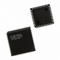
SCC68681E1A44,512 NXP Semiconductors, SCC68681E1A44,512 Datasheet - Page 21

SCC68681E1A44,512
Manufacturer Part Number
SCC68681E1A44,512
Description
IC DUART 44PLCC
Manufacturer
NXP Semiconductors
Datasheet
1.SCC68681C1A44512.pdf
(29 pages)
Specifications of SCC68681E1A44,512
Features
False-start Bit Detection
Number Of Channels
2, DUART
Fifo's
3Bit
Voltage - Supply
5V
With Auto Flow Control
Yes
With False Start Bit Detection
Yes
With Cmos
Yes
Mounting Type
Surface Mount
Package / Case
44-LCC (J-Lead)
Lead Free Status / RoHS Status
Lead free / RoHS Compliant
Other names
935274496512
SCC68681E1A44
SCC68681E1A44
SCC68681E1A44
SCC68681E1A44
Available stocks
Company
Part Number
Manufacturer
Quantity
Price
Company:
Part Number:
SCC68681E1A44,512
Manufacturer:
NXP Semiconductors
Quantity:
10 000
1. Parameters are valid over specified temperature range. See Ordering information table for applicable operating temperature and V
2. All voltage measurements are referenced to ground (GND). For testing, all inputs except X1/CLK swing between 0.4 V and 2.4 V with
3. Typical values are at +25 C, typical supply voltages, and typical processing parameters.
4. Test conditions for outputs: C
5. This specification will impose maximum 68000 CPU CLK to 6MHz. Higher CPU CLK can be used if repeating bus reads are not performed.
6. This specification imposes a lower bound on CSN and IACKN LOW, guaranteeing that it will be LOW for at least 1 CLK period. This
7. This spec is made only to insure that DTACKN is asserted with respect to the rising edge of the X1/CLK pin as shown in the timing diagram,
8. Operation to 0 MHz is assured by design. Minimum test frequency is 2.0 MHz.
Philips Semiconductors
AC CHARACTERISTICS
T
NOTES:
2004 Apr 06
amb
SYMBOL
SYMBOL
Reset Timing (See Figure 3)
Bus Timing (See Figures 4, 5, 6)
Port Timing (See Figure 7)
Interrupt Reset Timing (See Figure 9)
Clock Timing (See Figure 8)
Transmitter Timing (See Figure 10)
Receiver Timing (See Figure 11)
Dual asynchronous receiver/transmitter (DUART)
range.
a transition time of 20 ns maximum. For X1/CLK this swing is between 0.4 V and 4.4 V. All time measurements are referenced at input
voltages of 0.8 V and 2.0 V as appropriate.
Consecutive write operations to the same command register require at least three edges of the X1 clock between writes.
requirement is made on CSN only to insure assertion of DTACKN and not to guarantee operation of the part.
not to guarantee operation of the part. If setup time is violated, DTACKN may be asserted as shown, or may be asserted 1 clock cycle later.
t
t
t
t
t
t
t
t
t
t
t
t
t
t
t
t
t
t
t
t
t
t
f
t
f
t
f
t
f
t
t
t
t
RES
AS
AH
RWS
RWH
CSW
CSD
DD
DF
DS
DH
DAL
DCR
DCW
DAH
DAT
CSC
PS
PH
PD
IR
IR
CLK
CLK
CTC
CTC
RX
RX
RX
TX
TX
TX
TXD
TCS
RXS
RXH
= –40 C to +85 C; V
8
5
6
RESETN pulse width
A1–A4 setup time to CSN LOW
A1–A4 hold time from CSN LOW
RWN setup time to CSN HIGH
RWN hold time to CSN HIGH
CSN HIGH pulse width
CSN or IACKN HIGH from DTACKN LOW
Data valid from CSN or IACKN LOW
Data bus floating from CSN or IACKN HIGH
Data setup time to CLK HIGH
Data hold time from CSN HIGH
DTACKN LOW from read data valid
DTACKN LOW (read cycle) from CLK HIGH
DTACKN LOW (write cycle) from CLK HIGH
DTACKN HIGH from CSN or IACKN HIGH
DTACKN HIGH impedance from CSN or IACKN HIGH
CSN or IACKN setup time to clock HIGH
Port input setup time to CSN LOW
Port input hold time from CSN HIGH
Port output valid from CSN HIGH
INTRN or OP3–OP7 when used as interrupts negated from:
X1/CLK HIGH or LOW time
X1/CLK frequency
CTCLK HIGH or LOW time
CTCLK frequency
RxC HIGH or LOW time
RxC frequency
TxC HIGH or LOW time
TxC frequency
TxD output delay from TxC external clock input on IP pin
Output delay from TxC LOW at OP pin to TxD data output
RxD data setup time before RxC HIGH at external clock input on IP pin
RxD data hold time after RxC HIGH at external clock input on IP pin
Read RHR (RxRDY/FFULL interrupt)
Write THR (TxRDY interrupt)
Reset command (delta break interrupt)
Stop C/T command (counter interrupt)
Read IPCR (input port change interrupt)
Write IMR (clear of interrupt mask bit)
CC
= 5.0 V
L
1, 2, 3, 4
= 150 pF, except interrupt outputs. Test condition for interrupt outputs: C
(16 )
(1 )
(16 )
(1 )
10%
PARAMETER
PARAMETER
7
21
Min
200
100
100
100
100
220
220
240
200
90
20
20
90
10
0
0
–
–
0
–
–
–
–
0
0
–
–
–
–
–
–
–
0
0
0
0
0
0
–
–
L
= 50 pF, R
LIMITS
3.6864
Typ
–
–
–
–
–
–
–
–
–
–
–
–
–
–
–
–
–
–
–
–
–
–
–
–
–
–
–
–
–
–
–
–
–
–
–
–
–
–
3
L
= 2.7 k to V
SCC68681
Max
175
100
125
125
100
125
400
300
300
300
300
300
300
350
150
4.0
4.0
2.0
1.0
2.0
1.0
–
–
–
–
–
–
–
–
–
–
–
–
–
–
–
–
–
–
Product data
CC
CC
UNIT
UNIT
MHz
MHz
MHz
MHz
MHz
MHz
.
ns
ns
ns
ns
ns
ns
ns
ns
ns
ns
ns
ns
ns
ns
ns
ns
ns
ns
ns
ns
ns
ns
ns
ns
ns
ns
ns
ns
ns
ns
ns
ns
ns
ns
supply


