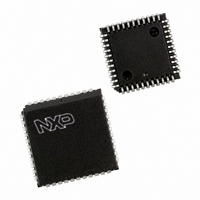
SCC68681E1A44,512 NXP Semiconductors, SCC68681E1A44,512 Datasheet - Page 9

SCC68681E1A44,512
Manufacturer Part Number
SCC68681E1A44,512
Description
IC DUART 44PLCC
Manufacturer
NXP Semiconductors
Datasheet
1.SCC68681C1A44512.pdf
(29 pages)
Specifications of SCC68681E1A44,512
Features
False-start Bit Detection
Number Of Channels
2, DUART
Fifo's
3Bit
Voltage - Supply
5V
With Auto Flow Control
Yes
With False Start Bit Detection
Yes
With Cmos
Yes
Mounting Type
Surface Mount
Package / Case
44-LCC (J-Lead)
Lead Free Status / RoHS Status
Lead free / RoHS Compliant
Other names
935274496512
SCC68681E1A44
SCC68681E1A44
SCC68681E1A44
SCC68681E1A44
Available stocks
Company
Part Number
Manufacturer
Quantity
Price
Company:
Part Number:
SCC68681E1A44,512
Manufacturer:
NXP Semiconductors
Quantity:
10 000
*These status bits are appended to the corresponding data character in the receive FIFO. A read of the status provides these bits (7:5) from the
*Add 0.5 to values shown for 0 - 7 if channel is programmed for 5 bits/char.
The level at the OP pin is the inverse of the bit in the OPR register.
Philips Semiconductors
Table 2.
NOTE:
* In block error mode, block error conditions must be cleared by using the error reset command (command 4x) or a receiver reset.
** Please see Receiver Reset note on page 19.
NOTE:
NOTE:
* See Table 6 for BRG Test frequencies in this data sheet, and “Extended baud rates for SCN2681, SCN68681, SCC2691, SCC2692,
SCC68681 and SCC2698B” in application notes elsewhere in this publication
NOTE:
*Access to the upper four bits of the command register should be separated by three (3) edges of the X1 clock. A disabled transmitter cannot
be loaded. For Rx and Tx performing a Disable and Enable at the same time results in Disable.
NOTE:
top of the FIFO together with bits (4:0). These bits are cleared by a ‘reset error status’ command. In character mode they are discarded when
the corresponding data character is read from the FIFO. In block error mode, block error conditions must be cleared by using the error reset
command (command 4x) or a receiver reset.
NOTE:
2004 Apr 06
OPR bit
OP pin
Dual asynchronous receiver/transmitter (DUART)
OPR
MR1A
MR1A
MR1B
MR2A
MR2A
MR2B
CSRA
CSRA
CSRB
CSRB
OPCR
CRA
CRB
CRB
SRA
SRB
SRB
0
1
Register Bit Formats
BIT 7
0 = OPR[7]
1 = TxRDYB
RECEIVED
BIT 7
CONTROL
Not used –
must be 0
BREAK*
0 = No
1 = Yes
RxRTS
BIT 7
BIT 7
0 = No
1 = Yes
1
0
OP7
BIT 7
BIT 7
BIT 7
CHANNEL MODE
00 = Normal
01 = Auto-Echo
10 = Local loop
11 = Remote loop
0
1
BIT 6
RECEIVER CLOCK SELECT
0 = OPR[6]
1 = TxRDYA
FRAMING
ERROR*
BIT 6
0 = RxRDY
1 = FFULL
0 = No
1 = Yes
MISCELLANEOUS COMMANDS
BIT 6
BIT 6
SELECT
OP6
BIT 6
1
0
RxINT
BIT 6
BIT 6
See Text
0
1
BIT 5
1 = RxRDY/
See Text
0 = OPR[5]
BIT 5
ERROR*
PARITY
0 = No
1 = Yes
BIT 5
BIT 5
BIT 5
OP5
FFULLB
0 = Char
1 = Block
CONTROL
1
0
ERROR
MODE*
0 = No
1 = Yes
BIT 5
TxRTS
BIT 5
0
1
BIT 4
1 = RxRDY/
0 = OPR[4]
BIT 4
OVERRUN
BIT 4
ERROR
0 = No
1 = Yes
BIT 4
BIT 4
OP4
FFULLA
9
1
0
BIT 4
ENABLE Tx
00 = With Parity
01 = Force Parity
10 = No Parity
11 = Multidrop Mode**
PARITY MODE
0 = No
1 = Yes
BIT 4
DISABLE Tx
CTS
0 = No
1 = Yes
0
1
BIT 3
BIT 3
TxEMT
0 = No
1 = Yes
BIT 3
BIT 3
00 = OPR[3]
01 = C/T OUTPUT
10 = TxCB(1 )
11 = RxCB(1 )
BIT 3
BIT 3
1
0
0 = 0.563
1 = 0.625
2 = 0.688
3 = 0.750
BIT 3
OP3
ENABLE Tx
TRANSMITTER CLOCK SELECT
0
1
0 = No
1 = Yes
BIT 2
BIT 2
BIT 2
TxRDY
0 = No
1 = Yes
BIT 2
0 = Even
BIT 2
PARITY
1 = Odd
TYPE
BIT 2
4 = 0.813
5 = 0.875
6 = 0.938
7 = 1.000
1
0
BIT 2
STOP BIT LENGTH*
See Text
DISABLE Rx
0
1
0 = No
1 = Yes
BIT 1
BIT 1
BIT 1
FFULL
0 = No
1 = Yes
BIT 1
BIT 1
8 = 1.563
9 = 1.625
A = 1.688
B = 1.750
BIT 1
BIT 1
00 = OPR[2]
01 = TxCA(16 )
10 = TxCA(1 )
11 = RxCA(1 )
SCC68681
1
0
CHARACTER
BITS PER
OP2
00 = 5
01 = 6
10 = 7
11 = 8
ENABLE Rx
0
1
BIT 0
Product data
C = 1.813
D = 1.875
E = 1.938
F = 2.000
BIT 0
0 = No
1 = Yes
BIT 0
RxRDY
BIT 0
0 = No
1 = Yes
BIT 0
BIT 0
BIT 0
1
0


