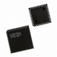
SCC68681E1A44,512 NXP Semiconductors, SCC68681E1A44,512 Datasheet - Page 4

SCC68681E1A44,512
Manufacturer Part Number
SCC68681E1A44,512
Description
IC DUART 44PLCC
Manufacturer
NXP Semiconductors
Datasheet
1.SCC68681C1A44512.pdf
(29 pages)
Specifications of SCC68681E1A44,512
Features
False-start Bit Detection
Number Of Channels
2, DUART
Fifo's
3Bit
Voltage - Supply
5V
With Auto Flow Control
Yes
With False Start Bit Detection
Yes
With Cmos
Yes
Mounting Type
Surface Mount
Package / Case
44-LCC (J-Lead)
Lead Free Status / RoHS Status
Lead free / RoHS Compliant
Other names
935274496512
SCC68681E1A44
SCC68681E1A44
SCC68681E1A44
SCC68681E1A44
Available stocks
Company
Part Number
Manufacturer
Quantity
Price
Company:
Part Number:
SCC68681E1A44,512
Manufacturer:
NXP Semiconductors
Quantity:
10 000
Philips Semiconductors
2004 Apr 06
SYMBOL
SYMBOL
X1/CLK
X2
RxDA
RxDB
TxDA
TxDB
OP0
OP1
OP2
OP3
OP4
OP5
OP6
OP7
IP0
IP1
IP2
IP3
IP4
IP5
V
GND
NC
CC
Dual asynchronous receiver/transmitter (DUART)
PLCC44
23, 34
1, 12,
36
37
35
33
13
32
14
31
15
30
16
29
17
40
43
42
44
22
11
8
5
3
PIN
DIP40
32
33
31
10
30
11
29
12
28
13
27
14
26
15
36
39
38
40
20
7
4
2
–
TYPE
TYPE
O
O
O
O
O
O
O
O
O
O
–
I
I
I
I
I
I
I
I
I
I
I
I
Output 2: General purpose output, or Channel A transmitter 1 or 16 clock output, or Channel A
Crystal 1: Crystal connection or an external clock input. A crystal of a clock the appropriate
frequency (nominally 3.6864 MHz) must be supplied at all times. For crystal connections see
Figure 8, Clock Timing.
Crystal 2: Crystal connection. See Figure 8. If a crystal is not used it is best to keep this pin not
connected. It must not be grounded.
Channel A Receiver Serial Data Input: The least significant bit is received first. ‘Mark’ is HIGH,
‘space’ is LOW.
Channel B Receiver Serial Data Input: The least significant bit is received first. ‘Mark’ is HIGH,
‘space’ is LOW.
Channel A Transmitter Serial Data Output: The least significant bit is transmitted first. This
output is held in the ‘mark’ condition when the transmitter is disabled, idle or when operating in
local loopback mode. ‘Mark’ is HIGH, ‘space’ is LOW.
Channel B Transmitter Serial Data Output: The least significant bit is transmitted first. This
output is held in the ‘mark’ condition when the transmitter is disabled, idle, or when operating in
local loopback mode. ‘Mark’ is HIGH, ‘space’ is LOW.
Output 0: General purpose output or Channel A request to send (RTSAN, active-LOW). Can be
deactivated automatically on receive or transmit.
Output 1: General purpose output or Channel B request to send (RTSBN, active-LOW). Can be
deactivated automatically on receive or transmit.
receiver 1 clock output.
Output 3: General purpose output or open-drain, active-LOW counter/timer interrupt output or
Channel B transmitter 1 clock output, or Channel B receiver 1 clock output.
Output 4: General purpose output or Channel A open-drain, active-LOW, RxRDYA/FFULLA
interrupt output.
Output 5: General purpose output or Channel B open-drain, active-LOW, RxRDYB/FFULLB
interrupt output.
Output 6: General purpose output or Channel A open-drain, active-LOW, TxRDYA interrupt
output.
Output 7: General purpose output, or Channel B open-drain, active-LOW, TxRDYB interrupt
output.
Input 0: General purpose input or Channel A clear to send active-LOW input (CTSAN). Pin has
an internal V
Input 1: General purpose input or Channel B clear to send active-LOW input (CTSBN). Pin has
an internal V
Input 2: General purpose input, or Channel B receiver external clock input (RxCB), or
counter/timer external clock input. When the external clock is used by the receiver, the received
data is sampled on the rising edge of the clock. Pin has an internal V
1 to 4 A of current.
Input 3: General purpose input or Channel A transmitter external clock input (TxCA). When the
external clock is used by the transmitter, the transmitted data is clocked on the falling edge of the
clock. Pin has an internal V
Input 4: General purpose input or Channel A receiver external clock input (RxCA). When the
external clock is used by the receiver, the received data is sampled on the rising edge of the
clock. Pin has an internal V
Input 5: General purpose input or Channel B transmitter external clock input (TxCB). When the
external clock is used by the transmitter, the transmitted data is clocked on the falling edge of the
clock. Pin has an internal V
Power Supply: +5 V supply input.
Ground.
Not connected.
CC
CC
pull-up device supplying 1 to 4 A of current.
pull-up device supplying 1 to 4 A of current.
4
CC
CC
CC
pull-up device supplying 1 to 4 A of current.
pull-up device supplying 1 to 4 A of current.
pull-up device supplying 1 to 4 A of current.
NAME AND FUNCTION
NAME AND FUNCTION
CC
pull-up device supplying
SCC68681
Product data


