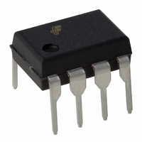
NM24C03N Fairchild Semiconductor, NM24C03N Datasheet

NM24C03N
Specifications of NM24C03N
Related parts for NM24C03N
NM24C03N Summary of contents
Page 1
... LOGIC SLAVE ADDRESS COMPARATOR SCL © 1998 Fairchild Semiconductor Corporation NM24C02/03 Rev Extended operating voltage 2.7V – 5.5V I 400 KHz clock frequency (F) at 2.7V - 5.5V I 200µA active current typical 10µA standby current typical 1µA standby current typical (L) 0.1µA standby current typical (LZ) ...
Page 2
A0,A1,A2 Device Address Inputs V Ground SS SDA Serial Data I/O SCL Serial Clock Input NC No Connection V Power Supply CC A0,A1,A2 Device Address Inputs V Ground SS SDA Serial Data I/O SCL Serial Clock input WP Write Protect ...
Page 3
NM24C02/03 Rev XXX Letter Description N 8-pin DIP M8 8-pin SOIC MT8 8-pin TSSOP None 0 to 70°C V -40 to +125°C E -40 to +85°C Blank 4.5V to 5.5V L 2.7V to ...
Page 4
Ambient Storage Temperature All Input or Output Voltages with Respect to Ground Lead Temperature (Soldering, 10 seconds) ESD Rating I Active Power Supply Current f CCA I Standby Current SB I Input Leakage Current LI I Output Leakage Current LO ...
Page 5
Input Pulse Levels V CC Input Rise and Fall Times 10 ns Input & Output Timing Levels V CC Output Load 1 TTL Gate and C f SCL Clock Frequency SCL T Noise Suppression Time Constant at I SCL, SDA ...
Page 6
SCL SDA 8th BIT WORD n The write cycle time ( the time from a valid stop condition of a write sequence to the end of the internal erase/program cycle. WR SDA SCL Master Transmitter/ Receiver Due to ...
Page 7
... Since each page is 2K bit in size bit = 16K bit is the maximum size of memory that is addressable on the Standard IIC bus. This 16Kb of memory can be in the form of a single 16Kb EEPROM device or multiple EEPROMs of varying density (in 2Kb multiples maximum total of 16Kb. To address the needs of systems that require more than 16Kb on the IIC bus, a different specification called “ ...
Page 8
... READ/ SS WRITE over the entire memory is possible. This feature allows the user to assign the upper half of the memory as ROM which can be protected against accidental programming. When write is disabled, slave address and word address will be acknowledged but data will not be acknowledged. ...
Page 9
SCL SDA SCL SDA START CONDITION SCL FROM MASTER DATA OUTPUT FROM TRANSMITTER DATA OUTPUT FROM RECEIVER START CONDITION NM24C02/03 Rev. G DATA STABLE DATA CHANGE CONDITION DS500069-10 STOP DS500069- ACKNOWLEDGE PULSE DS500069-12 ...
Page 10
The NM24C02/03 device will always respond with an acknowl- edge after recognition of a start condition and its slave address. If both the device and a write operation have been selected, the NM24C02/03 will respond with an acknowledge after the ...
Page 11
... For a write operation a second address field is required which is a word address that is comprised of eight bits and provides access to any one of the 256 bytes in the selected page of memory. Upon receipt of the byte address the NM24C02/03 responds with an acknowledge and waits for the next eight bits of data, again, responding with an acknowledge ...
Page 12
... After the entire memory has been read, the counter "rolls over" to the beginning of the memory. NM24C02/03 continues to output data for each acknowledge received. Refer to Figure 8 for the address, acknowledge, and data transfer sequence ...
Page 13
All lead tips Typ. All Leads 0.114 - 0.122 (2.90 - 3.10) 8 ...
Page 14
... Fairchild's products are not authorized for use as critical components in life support devices or systems without the express written approval of the President of Fairchild Semiconductor Corporation. As used herein: 1. Life support devices or systems are devices or systems which, (a) are intended for surgical implant into the body, or (b) support ...


