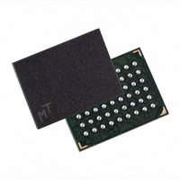
MT45W4MW16BFB-706 WT TR Micron Technology Inc, MT45W4MW16BFB-706 WT TR Datasheet - Page 13

MT45W4MW16BFB-706 WT TR
Manufacturer Part Number
MT45W4MW16BFB-706 WT TR
Description
IC PSRAM 64MBIT 70NS 54VFBGA
Manufacturer
Micron Technology Inc
Datasheet
1.MT45W4MW16BBB-706_WT_TR.pdf
(61 pages)
Specifications of MT45W4MW16BFB-706 WT TR
Format - Memory
RAM
Memory Type
PSRAM (Page)
Memory Size
64M (4M x 16)
Speed
70ns
Interface
Parallel
Voltage - Supply
1.7 V ~ 1.95 V
Operating Temperature
-30°C ~ 85°C
Package / Case
54-VFBGA
Lead Free Status / RoHS Status
Contains lead / RoHS non-compliant
Mixed-Mode Operation
WAIT Operation
Figure 10:
PDF: 09005aef80be1fbd/Source: 09005aef80be2036
Burst CellularRAM_2.fm - Rev. G 10/05 EN
Wired or WAIT Configuration
The device can support a combination of synchronous READ and asynchronous WRITE
operations when the BCR is configured for synchronous operation. The asynchronous
READ and WRITE operations require that the clock (CLK) remain static (HIGH or LOW)
during the entire sequence. The ADV# signal can be used to latch the target address, or it
can remain LOW during the entire WRITE operation. CE# must return HIGH when tran-
sitioning between mixed-mode operations. Note that the
READ or WRITE cycle. This time is required to ensure adequate refresh. Mixed-mode
operation facilitates a seamless interface to legacy burst mode Flash memory control-
lers. See Figure 42 on page 53 for the “Asynchronous WRITE Followed by Burst READ”
timing diagram.
The WAIT output on a CellularRAM device is typically connected to a shared, system-
level WAIT signal (see Figure 10). The shared WAIT signal is used by the processor to
coordinate transactions with multiple memories on the synchronous bus.
Once a READ or WRITE operation has been initiated, WAIT goes active to indicate that
the CellularRAM device requires additional time before data can be transferred. For
READ operations, WAIT will remain active until valid data is output from the device. For
WRITE operations, WAIT will indicate to the memory controller when data will be
accepted into the CellularRAM device. When WAIT transitions to an inactive state, the
data burst will progress on successive clock edges.
CE# must remain asserted during WAIT cycles (WAIT asserted and WAIT configuration
BCR[8] = 1). Bringing CE# HIGH during WAIT cycles may cause data corruption. (Note
that for BCR[8] = 0, the actual WAIT cycles end one cycle after WAIT de-asserts, and for
row boundary crossings, start one cycle after the WAIT signal asserts.)
The WAIT output also performs an arbitration role when a READ or WRITE operation is
launched while an on-chip refresh is in progress. If a collision occurs, WAIT is asserted
for additional clock cycles until the refresh has completed (see Figures 11 and 12 on
page 15). When the REFRESH operation has completed, the READ or WRITE operation
will continue normally.
WAIT is also asserted when a continuous READ or WRITE burst crosses a row boundary.
The WAIT assertion allows time for the new row to be accessed, and permits any pend-
ing REFRESH operations to be performed.
Processor
READY
64Mb: 4 Meg x 16 Async/Page/Burst CellularRAM 1.0 Memory
WAIT
Device
Other
CellularRAM
WAIT
13
WAIT
Device
Other
Micron Technology, Inc., reserves the right to change products or specifications without notice.
External
Pull-Up/
Pull-Down
Resistor
t
CKA period is the same as a
Bus Operating Modes
©2003 Micron Technology, Inc. All rights reserved.


