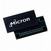
MT47H64M8CB-3:B Micron Technology Inc, MT47H64M8CB-3:B Datasheet - Page 107

MT47H64M8CB-3:B
Manufacturer Part Number
MT47H64M8CB-3:B
Description
IC DDR2 SDRAM 512MBIT 3NS 60FBGA
Manufacturer
Micron Technology Inc
Datasheet
1.MT47H64M8CB-5EB.pdf
(133 pages)
Specifications of MT47H64M8CB-3:B
Format - Memory
RAM
Memory Type
DDR2 SDRAM
Memory Size
512M (64M x 8)
Speed
3ns
Interface
Parallel
Voltage - Supply
1.7 V ~ 1.9 V
Operating Temperature
0°C ~ 85°C
Package / Case
60-FBGA
Lead Free Status / RoHS Status
Lead free / RoHS Compliant
Available stocks
Company
Part Number
Manufacturer
Quantity
Price
Company:
Part Number:
MT47H64M8CB-3:B
Manufacturer:
MICRON
Quantity:
12 388
Company:
Part Number:
MT47H64M8CB-3:B
Manufacturer:
Micron Technology Inc
Quantity:
10 000
Company:
Part Number:
MT47H64M8CB-3:B TR
Manufacturer:
Micron Technology Inc
Quantity:
10 000
Table 38:
Table 39:
Figure 83:
PDF: 09005aef8117c18e, Source: 09005aef8211b2e6
512MbDDR2_2.fm - Rev. K 8/06 EN
Output DC Current Drive
Output Characteristics
Output Slew Rate Load
Notes:
Notes:
1. For I
2. For I
3. The DC value of V
4. The values of I
1. Absolute specifications: 0°C ≤ T
2. Impedance measurement conditions for output source DC current: V
3. Mismatch is absolute value between pull-up and pull-down; both are measured at same
4. Output slew rate for falling and rising edges is measured between V
5. The absolute value of the slew rate as measured from V
6. IT devices require an additional 0.4 V/ns in the MAX limit when T
Output
(V
Parameter
Parameter
Output minimum source DC current
Output minimum sink DC current
Output impedance
Pull-up and Pull-down mismatch
Output slew rate
OUT
ues of V
between 0V and 280mV.
are used to test device drive current capability to ensure V
V
ues are derived by shifting the desired driver operating point (see output IV curves) along a
21
1,420mV; (V
V
V
temperature and voltage.
250mV for single-ended signals. For differential signals (DQS - DQS#), output slew rate is
measured between DQS - DQS# = –500mV and DQS# - DQS = +500mV. Output slew rate is
guaranteed by design, but is not necessarily tested on each device.
or greater than the slew rate as measured from V
teed by design and characterization.
0°C.
IL
DD
OUT
)
V
Ω
TT =
(MAX) minus a noise margin are delivered to an SSTL_18 receiver. The actual current val-
Q - 280mV. Impedance measurement condition for output sink DC current: V
OH
OL
load line to define a convenient driver current for measurement.
= 280mV; V
V
(
(
DC
DD
DC
OUT
25Ω
Output Electrical Characteristics and Operating Conditions
); V
Reference
Point
Q/2
); V
OUT
between V
DD
DD
OH
Q = 1.7V, V
Q = 1.7V, V
- V
OUT
(
DC
REF
DD
) and I
/I
Q)/I
applied to the receiving device is set to V
OL
DD
must be less than 23.4
OH
Q and V
OUT
OL
OUT
107
must be less than 23.4
(
DC
= 280mV. V
= 1,420mV. (V
C
See “Full Strength Pull-Down Driver
) are based on the conditions given in Notes 1 and 2. They
≤ +85°C
DD
Min
Characteristics” on page 108
1.5
Q - 280mV.
0
Micron Technology, Inc., reserves the right to change products or specifications without notice.
Symbol
;
OUT
V
I
I
DD
OH
OL
OUT
/I
512Mb: x4, x8, x16 DDR2 SDRAM
Q = +1.8V ±0.1V, V
Ω
OL
Nom
- V
for values of V
must be less than 21
IL
Ω
(
DD
AC
for values of V
Q)/I
) MAX to V
Value
–13.4
IL
13.4
(
DC
OH
IH
Max
) MAX to V
must be less than 21
(MIN) plus a noise margin and
4
5
TT
OUT
©2004 Micron Technology, Inc. All rights reserved.
DD
.
IH
C
(
is between –40°C and
OUT
= +1.8V ±0.1V.
between 0V and 280mV.
AC
Units
DD
TT
mA
mA
Ω
) MIN. This is guaran-
IH
Units
Q = 1.7V; V
- 250mV and V
between V
V/ns
(
for values of V
DC
Ω
Ω
) MIN is equal to
DD
Notes
Ω
1, 2, 4
2, 3, 4
1, 4, 5, 6
OUT
DD
Q = 1.7V;
Notes
1, 2, 3
for val-
1, 2
Q and
TT
=
OUT
+


