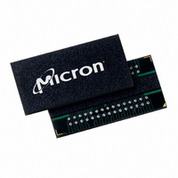
MT47H64M8CB-3:B Micron Technology Inc, MT47H64M8CB-3:B Datasheet - Page 7

MT47H64M8CB-3:B
Manufacturer Part Number
MT47H64M8CB-3:B
Description
IC DDR2 SDRAM 512MBIT 3NS 60FBGA
Manufacturer
Micron Technology Inc
Datasheet
1.MT47H64M8CB-5EB.pdf
(133 pages)
Specifications of MT47H64M8CB-3:B
Format - Memory
RAM
Memory Type
DDR2 SDRAM
Memory Size
512M (64M x 8)
Speed
3ns
Interface
Parallel
Voltage - Supply
1.7 V ~ 1.9 V
Operating Temperature
0°C ~ 85°C
Package / Case
60-FBGA
Lead Free Status / RoHS Status
Lead free / RoHS Compliant
Available stocks
Company
Part Number
Manufacturer
Quantity
Price
Company:
Part Number:
MT47H64M8CB-3:B
Manufacturer:
MICRON
Quantity:
12 388
Company:
Part Number:
MT47H64M8CB-3:B
Manufacturer:
Micron Technology Inc
Quantity:
10 000
Company:
Part Number:
MT47H64M8CB-3:B TR
Manufacturer:
Micron Technology Inc
Quantity:
10 000
Part Numbers
Figure 1:
FBGA Part Marking Decoder
General Description
PDF: 09005aef8117c18e, Source: 09005aef8211b2e6
512MbDDR2_2.fm - Rev. K 8/06 EN
512Mb DDR2 Part Numbers
Note:
Due to space limitations, FBGA-packaged components have an abbreviated part
marking that is different from the part number. Micron’s FBGA Part Marking Decoder is
available at
The 512Mb DDR2 SDRAM is a high-speed CMOS, dynamic random access memory
containing 536,870,912 bits. It is internally configured as a 4-bank DRAM. The functional
block diagrams of the all device configurations are shown in “Functional Description”
on page 14. Ball assignments and signal descriptions are shown in “Ball Assignment and
Description” on page 9.
The 512Mb DDR2 SDRAM uses a double data rate architecture to achieve high-speed
operation. The double data rate architecture is essentially a 4n-prefetch architecture,
with an interface designed to transfer two data words per clock cycle at the I/O balls. A
single read or write access for the 512Mb DDR2 SDRAM effectively consists of a single
4n-bit-wide, one-clock-cycle data transfer at the internal DRAM core and four corre-
sponding n-bit-wide, one-half-clock-cycle data transfers at the I/O balls.
A bidirectional data strobe (DQS, DQS#) is transmitted externally, along with data, for
use in data capture at the receiver. DQS is a strobe transmitted by the DDR2 SDRAM
during READs and by the memory controller during WRITEs. DQS is edge-aligned with
data for READs and center-aligned with data for WRITEs. The x16 offering has two data
strobes, one for the lower byte (LDQS, LDQS#) and one for the upper byte (UDQS,
UDQS#).
Not all speeds and configurations are available. Contact Micron sales for current revision.
Configuration
MT47H
128 Meg x 4
32 Meg x 16
64 Meg x 8
Package
84-Ball 12 x 12.5 FBGA
84-Ball 10 x 12.5 FBGA
60-Ball 12 x 10 FBGA
60-Ball 10 x 10 FBGA
Example Part Number: M T 4 7 H6 4M 8B T-3 7 E : A
www.micron.com/decoder.
Configuration
128M4
32M16
64M8
Package
CC
BN
CB
B6
7
-
Speed
-37E
-25E
Micron Technology, Inc., reserves the right to change products or specifications without notice.
-5E
-3E
-25
-3
L
IT
Low-Power
Industrial Temperature
t CK = 5ns, CL = 3
t CK = 3.75ns, CL = 4
t CK = 3ns, CL = 5
t CK = 3ns, CL = 4
t CK = 2.5ns, CL = 6
t CK = 2.5ns, CL = 5
512Mb: x4, x8, x16 DDR2 SDRAM
Speed Grade
:A/:B/:D
Revision
:
Revision
©2004 Micron Technology, Inc. All rights reserved.
Part Numbers


