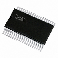
PCF8566T/1,118 NXP Semiconductors, PCF8566T/1,118 Datasheet - Page 16

PCF8566T/1,118
Manufacturer Part Number
PCF8566T/1,118
Description
IC LCD DVR UNVRSL LOW-MUX 40VSOP
Manufacturer
NXP Semiconductors
Datasheet
1.PCF8566T1118.pdf
(48 pages)
Specifications of PCF8566T/1,118
Package / Case
40-VSOP
Display Type
LCD
Configuration
7 Segment + DP, 14 Segment (24 Segment)
Interface
I²C
Current - Supply
30µA
Voltage - Supply
2.5 V ~ 6 V
Operating Temperature
-40°C ~ 85°C
Mounting Type
Surface Mount
Number Of Digits
12
Number Of Segments
96
Maximum Clock Frequency
315 KHz
Operating Supply Voltage
2.5 V to 6 V
Maximum Power Dissipation
400 mW
Maximum Operating Temperature
+ 85 C
Maximum Supply Current
90 uA
Minimum Operating Temperature
- 40 C
Lead Free Status / RoHS Status
Lead free / RoHS Compliant
Digits Or Characters
-
Lead Free Status / Rohs Status
Lead free / RoHS Compliant
Other names
568-1070-2
935278688118
PCF8566TD-T
935278688118
PCF8566TD-T
NXP Semiconductors
PCF8566_7
Product data sheet
7.10 Backplane outputs
7.11 Display RAM
7.7 Display register
7.8 Shift register
7.9 Segment outputs
The lower clock frequency has the disadvantage of increasing the response time when
large amounts of display data are transmitted on the I
process a display data byte before the next one arrives, it holds the SCL line LOW until the
first display data byte is stored. This slows down the transmission rate of the I
no data loss occurs.
The display register holds the display data while the corresponding multiplex signals are
generated. There is a one-to-one relationship between the data in the display register, the
LCD segment outputs and one column of the display RAM.
The shift register transfers display information from the display RAM to the display register
while previous data is displayed.
The LCD drive section includes 24 segment outputs S0 to S23 which must be connected
directly to the LCD. The segment output signals are generated based on the multiplexed
backplane signals and with data resident in the display register. When less than
24 segment outputs are required, the unused segment outputs should be left open-circuit.
The LCD drive section includes four backplane outputs: BP0 to BP3. The backplane
output signals are generated based on the selected LCD drive mode.
If less than four backplane outputs are required the unused outputs can be left as an
open-circuit.
The display RAM is a static 24
map indicates the on-state of the corresponding LCD segment; similarly, logic 0 indicates
the off-state. There is a direct relationship between the RAM addresses and the segment
outputs, and between the individual bits of a RAM word and the backplane outputs. The
first RAM row corresponds to the 24 segments operated with respect to backplane BP0
(see
display RAM are time-multiplexed with BP0, BP1, BP2 and BP3 respectively.
•
•
•
•
In 1:4 multiplex drive mode: BP0 to BP3 must be connected directly to the LCD.
In 1:3 multiplex drive mode: BP3 carries the same signal as BP1, therefore these two
adjacent outputs can be tied together to give enhanced drive capabilities.
In 1:2 multiplex drive mode: BP0 and BP2, BP1 and BP3 respectively carry the same
signals and can also be paired to increase the drive capabilities.
In static drive mode: the same signal is carried by all four backplane outputs and they
can be connected in parallel for very high drive requirements.
Figure
10). In multiplexed LCD applications, the segment data of rows 1 to 4 of the
Rev. 07 — 25 February 2009
4-bit RAM which stores LCD data. Logic 1 in the RAM bit
Universal LCD driver for low multiplex rates
2
C-bus. When a device is unable to
PCF8566
© NXP B.V. 2009. All rights reserved.
2
C-bus but
16 of 48


