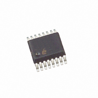
ISL6549CAZA-T Intersil, ISL6549CAZA-T Datasheet - Page 11

ISL6549CAZA-T
Manufacturer Part Number
ISL6549CAZA-T
Description
IC CTRLR PWM SYNC BUCK 16-QSOP
Manufacturer
Intersil
Datasheet
1.ISL6549CAZR5213.pdf
(18 pages)
Specifications of ISL6549CAZA-T
Pwm Type
Voltage Mode
Number Of Outputs
2
Frequency - Max
1MHz
Duty Cycle
100%
Voltage - Supply
4.75 V ~ 13.2 V
Buck
Yes
Boost
No
Flyback
No
Inverting
No
Doubler
No
Divider
No
Cuk
No
Isolated
No
Operating Temperature
0°C ~ 70°C
Package / Case
16-QSOP
Frequency-max
1MHz
Lead Free Status / RoHS Status
Lead free / RoHS Compliant
Other names
ISL6549CAZA-TTR
Available stocks
Company
Part Number
Manufacturer
Quantity
Price
Part Number:
ISL6549CAZA-T
Manufacturer:
INTERSIL
Quantity:
20 000
Use the following guidelines for locating the poles and zeros of
the compensation network:
1. Select a value for R1 (1kΩ to 5kΩ, typically). Calculate
2. Calculate C1 such that F
3. Calculate C2 such that F
FIGURE 10. VOLTAGE-MODE BUCK CONVERTER
value for R2 for desired converter bandwidth (F
setting the output voltage via an offset resistor connected
to the FB pin, Ro in Figure 10, the design procedure can
be followed as presented.
at 0.1 to 0.75 of F
desired number). The higher the quality factor of the output
filter and/or the higher the ratio F
frequency (to maximize phase boost at F
R2
C1
C2
CIRCUIT
PWM
=
=
=
-------------------------------------------- -
d
----------------------------------------------- -
2π R2 0.5 F
---------------------------------------------------------
2π R2 C1 F
V
MAX
COMP
OSC
⋅
⋅
COMPENSATION DESIGN
⋅
HALF-BRIDGE
V
⋅
⋅
⋅
OSCILLATOR
1
R1 F
V
IN
C1
OSC
E/A
DRIVE
⋅
LC
⋅
⋅
⋅
F
R2
LC
ISL6549
0
CE
(to adjust, change the 0.5 factor to
LC
C2
+
-
VREF
–
Z1
P1
1
C1
11
is placed at a fraction of the F
is placed at F
FB
UGATE
LGATE
PHASE
EXTERNAL CIRCUIT
CE
/F
R3
Ro
LC
V
IN
R1
, the lower the F
LC
CE
C3
L
).
.
V
0
D
OUT
). If
C
E
(EQ. 5)
(EQ. 6)
(EQ. 4)
LC
Z1
ISL6549
,
It is recommended a mathematical model is used to plot the
loop response. Check the loop gain against the error
amplifier’s open-loop gain. Verify phase margin results and
adjust as necessary. Equation 8 describes the frequency
response of the modulator (G
(G
COMPENSATION BREAK FREQUENCY EQUATIONS
Figure 11 shows an asymptotic plot of the DC-DC converter’s
gain vs. frequency. The actual Modulator Gain has a high gain
peak dependent on the quality factor (Q) of the output filter,
which is not shown. Using the above guidelines should yield a
compensation gain similar to the curve plotted. The open loop
error amplifier gain bounds the compensation gain. Check the
compensation gain at F
amplifier. The closed loop gain, G
log-log graph of Figure 11 by adding the modulator gain, G
(in dB), to the feedback compensation gain, G
equivalent to multiplying the modulator transfer function and the
compensation transfer function and then plotting the resulting
gain.
G
G
F
F
G
4. Calculate R3 such that F
Z1
Z2
MOD
FB
CL
FB
such that F
times F
Change the numerical factor to reflect desired placement
of this pole. Placement of F
reduce the gain of the compensation network at high
frequency, in turn reducing the HF ripple component at
the COMP pin and minimizing resultant duty cycle jitter.
R3
f ( )
f ( )
=
=
) and closed-loop response (G
f ( )
------------------------------- -
2π R2 C1
-------------------------------------------------- -
2π
=
=
=
⋅
=
----------------------------------------------------- - ⋅
s f ( ) R1
---------------------------------------------------------------------------------------------------------------------------- -
(
⋅
⋅
G
--------------------- -
F
----------- - 1
F
1
(
SW
1
SW
d
----------------------------- -
MOD
LC
R1
1
+
R1
MAX
+
⋅
s f ( ) R3 C3
V
⋅
P2
). F
s f ( ) R2 C1
+
–
1
OSC
f ( ) G
R3
⋅
is placed below F
⋅
⋅
SW
V
⋅
⋅
(
) C3
C1
IN
1
⋅
FB
+
represents the switching frequency.
⋅
⋅
P2
⋅
+
s f ( )
----------------------------------------------------------------------------------------
1
f ( )
C2
+
against the capabilities of the error
)
s f ( )
⋅
⋅
)
Z2
(
⎛
⎝
R1
1
MOD
C3
is placed at F
⋅
+
F
F
P2
(
P1
P2
1
+
CL
s f ( ) R2
E
=
where s f ( )
+
R3
), feedback compensation
+
SW
lower in frequency helps
, is constructed on the
=
=
-------------------------------------------------
2π R3 0.7 F
s f ( ) E C
CL
D
⋅
) C3
---------------------------------------------- -
2π R2
------------------------------- -
2π R3 C3
) C
⋅
(typically, 0.5 to 1.0
⋅
):
⋅
⋅
,
⋅
⋅
⋅
⎛
⎝
+
⋅
--------------------- -
C1
1
⋅
C1 C2
LC
1
s
FB
2
⋅
⋅
1
=
f ( ) L C
. Calculate C3
+
--------------------- -
C1
⋅
C1 C2
September 22, 2006
(in dB). This is
⋅
2π f j
C2
⋅
+
SW
⋅
⎞
⎠
⋅ ⋅
C2
⋅
⎞
⎠
(EQ. 8)
(EQ. 9)
FN9168.2
(EQ. 7)
MOD


