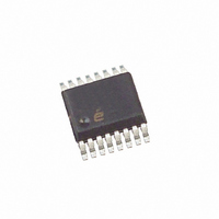
ISL6549CAZA-T Intersil, ISL6549CAZA-T Datasheet - Page 6

ISL6549CAZA-T
Manufacturer Part Number
ISL6549CAZA-T
Description
IC CTRLR PWM SYNC BUCK 16-QSOP
Manufacturer
Intersil
Datasheet
1.ISL6549CAZR5213.pdf
(18 pages)
Specifications of ISL6549CAZA-T
Pwm Type
Voltage Mode
Number Of Outputs
2
Frequency - Max
1MHz
Duty Cycle
100%
Voltage - Supply
4.75 V ~ 13.2 V
Buck
Yes
Boost
No
Flyback
No
Inverting
No
Doubler
No
Divider
No
Cuk
No
Isolated
No
Operating Temperature
0°C ~ 70°C
Package / Case
16-QSOP
Frequency-max
1MHz
Lead Free Status / RoHS Status
Lead free / RoHS Compliant
Other names
ISL6549CAZA-TTR
Available stocks
Company
Part Number
Manufacturer
Quantity
Price
Part Number:
ISL6549CAZA-T
Manufacturer:
INTERSIL
Quantity:
20 000
Functional Pin Description
VCC12
This is the power supply pin for the IC; it sources the internal
5V regulator used for the gate drivers. Provide a local
decoupling capacitor to GND. The voltage at this pin is
monitored for Power-On Reset (POR) purposes. The
16 Ld QFN and 16 Ld QSOP have two VCC12 pins; tie them
together on the board.
VCC5
This pin supplies the internal 5V bias for analog and logic
functions. Provide a local decoupling capacitor to GND, and a
resistor to PVCC. The voltage at this pin is monitored for
Power-On Reset (POR) purposes. See “Internal PVCC5
Regulator” on page 7 for more details.
GND, AGND, DGND
These pins are the signal ground for the IC. All voltage levels
are measured with respect to these pins. Connect all to the
ground plane via the shortest available path.
PVCC5
This pin is the internal 5V linear regulator for the BOOT supply
(for the UGATE driver), and the source for the LGATE.
Provide a local decoupling capacitor to PGND. Do not use this
pin as a voltage source for other circuits. See “Internal PVCC5
Regulator” on page 7 for more details.
PGND
This pin is the power ground return for the lower gate driver.
(LGATE). Connect to the ground plane on the board via the
shortest available path.
UGATE
This output pin drives the upper MOSFET gate from the
internal 5V regulator. Connect it to the gate of the upper
MOSFET via a short, low inductance trace.
BOOT
The BOOT pin, along with the external capacitor (from
PHASE to BOOT), an internal diode, and the internal 5.5V
regulator, creates the bootstrap voltage for the upper gate
driver (UGATE). The maximum voltage is around 5.5V (above
PHASE).
PHASE
This pin represents the return path for the upper gate drive.
Connect it to the source of the upper MOSFET via a short, low
inductance trace.
LGATE
This output pin drives the lower MOSFET gate from the
internal 5V regulator. Connect it to the gate of the lower
MOSFET via a short, low inductance trace.
6
ISL6549
FB
FB is the available external inverting input pin of the error
amplifier. Connect the output of the switching regulator to
this pin through a properly sized resistor divider, to set the
output voltage. The voltage at this pin is regulated to the
internal reference voltage. This pin is also monitored for
undervoltage detection.
COMP
COMP is the available external output pin of the error amplifier.
This pin is used to compensate the voltage-mode control
feedback loop of the standard synchronous rectified buck
converter. Connect an appropriate compensation network
between this and the FB pin. See “PWM Controller Feedback
Compensation” on page 10 for more information.
FS_DIS
This input pin has two functions. A resistor to GND sets the
internal oscillator frequency for the switching regulator. In
addition, if the pin is pulled down towards GND with a low
impedance (<1kΩ, such as an external FET), it will disable
both regulator outputs until released (at which time a new soft-
start cycle will begin).
LDO_DR
This output pin provides the gate voltage for the linear
regulator pass transistor. Connect this pin to the gate terminal
of an external N-channel MOSFET transistor. This pin (along
with the LDO_FB pin) also provides a means of compensating
the error amplifier, should the application require it.
LDO_FB
This input pin is the FB inverting input on the linear regulator
error amplifier. Connect the output of the linear regulator to
this pin through a properly sized resistor divider, to set the
output voltage. The voltage at this pin is regulated to the
internal reference voltage. This pin is also monitored for
undervoltage detection.
Bottom Pad (QFN Package Only)
The QFN package’s metal bottom pad is resistively tied to the
internal IC GND. For best thermal and electrical performance,
connect this pad to the GND pins, and to the ground plane of
the PCB through 4 vias equidistantly situated inside the solder
landing pad.
September 22, 2006
FN9168.2


