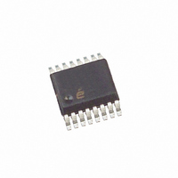
ISL6549CAZA-T Intersil, ISL6549CAZA-T Datasheet - Page 7

ISL6549CAZA-T
Manufacturer Part Number
ISL6549CAZA-T
Description
IC CTRLR PWM SYNC BUCK 16-QSOP
Manufacturer
Intersil
Datasheet
1.ISL6549CAZR5213.pdf
(18 pages)
Specifications of ISL6549CAZA-T
Pwm Type
Voltage Mode
Number Of Outputs
2
Frequency - Max
1MHz
Duty Cycle
100%
Voltage - Supply
4.75 V ~ 13.2 V
Buck
Yes
Boost
No
Flyback
No
Inverting
No
Doubler
No
Divider
No
Cuk
No
Isolated
No
Operating Temperature
0°C ~ 70°C
Package / Case
16-QSOP
Frequency-max
1MHz
Lead Free Status / RoHS Status
Lead free / RoHS Compliant
Other names
ISL6549CAZA-TTR
Available stocks
Company
Part Number
Manufacturer
Quantity
Price
Part Number:
ISL6549CAZA-T
Manufacturer:
INTERSIL
Quantity:
20 000
Description
Operation Overview
The ISL6549 monitors and precisely controls two output
voltage levels. Refer to the “Block Diagram” on page 2,
“Simplified Power System Diagram” on page 3, and “Typical
Application Schematic” on page 3. The controller is intended
for use in applications where only a 12V bias input is
available. The IC integrates both a standard buck PWM
controller and a linear controller. The PWM controller
regulates the output voltage (V
by a resistor divider. The linear controller is designed to
regulate the lower current local memory voltage (V
through an external N-Channel MOS pass transistor.
Internal PVCC5 Regulator
The preferred and recommended configuration is as follows:
+12V to VCC12 pin, a resistor (~10Ω) between PVCC5 and
VCC5 pins, and decoupling caps on all three pins to ground.
This creates the PVCC5 voltage for the gate drivers, and
externally filters it for bias on the VCC5 pin. It also guarantees
that all 3 voltages track each other during power-up and
power-down.
The PVCC5 pin cannot be used as an input and it should not
be used as an output for other circuits; its current capability is
reserved for the gate drivers and VCC5 bias. Similarly, the
VCC5 pin should not be used as an output. Although not
preferred, the VCC5 pin can be used with an external 5V
supply (±5%). However, proper precautions must be followed,
which mainly have to do with proper sequencing, to prevent
latch-up or related problems. Note in the power-up diagram
(Figure 1), the 5V lags the 12V by a few msecs and a volt or
so; that is expected. Both the VCC12 and VCC5 pins must
exceed their rising POR trip points before the soft-start is
enabled; the trip order is not important as long as both have
some voltage. The 12V can be present with no 5V at all, but
the 5V should not precede the 12V. Similarly, on power down,
the 5V should discharge with or before the 12V.
Under normal operation, the internal regulator can supply up
to 100mA (which includes the VCC5 bias current, with the
resistor between the pins). The amount of current is
determined primarily by the switching parameters: the
oscillator frequency and the loading of the FET gates.
Overloading of the internal regulator is not recommended;
even if there is enough current, the gate driver waveforms
may be degraded. See “Switcher FET Considerations” on
page 13 for more details.
The PVCC5 pin has a current limit that provides some
protection against a shorted gate driver dragging down the
12V rail. The temperature of the IC will increase as the current
and corresponding on-chip power dissipation increases.
There is no thermal shutdown, so even if the current limit is
effective, the IC can be subject to very high temperatures. If
the current limit is exceeded, the regulator voltage will likely
7
OUT1
) to a level programmed
OUT2
)
ISL6549
collapse, shutting down everything until the load current is
reduced or removed.
Initialization
The ISL6549 automatically initializes upon application of input
power (at the VCC12) pin. The ISL6549 creates its own
PVCC5 and VCC5 supplies for internal use. The POR
function continually monitors the input bias supply voltage at
the VCC12 and VCC5 pins. The POR function initiates soft-
start operation after both these supply voltages exceed their
POR rising threshold voltages.
Soft-Start
The POR function initiates the digital soft-start sequence. Both
the linear regulator error amplifier and PWM error amplifier
reference inputs are forced to track a voltage level
proportional to the soft-start voltage. As the soft-start voltage
slews up, the PWM comparator regulates the output relative
to the tracked soft-start voltage, slowly charging the output
capacitor(s). Simultaneously, the linear output follows the
smooth ramp of the soft-start function into normal regulation.
Figure 1 shows the soft-start sequence. Both the VCC12 and
VCC5 pins must be above their respective rising POR trip
points. In most cases, as shown here, the last one exceeding
its threshold is the VCC12 around 9.5V. The ramp time is
based on the internal oscillator period multiplied by 4096. So
for a 600kHz (1.67µs) example, the soft-start ramp time would
be 6.8ms.
Figure 2 shows more detail of the output ramps, by increasing
the time and voltage resolution. The clock for the DAC
producing the steps is approximately 9.4kHz (600kHz/64), so
each step is just over 100µs long. The step voltage is 1/64 of
the final value for each output; around 31mV for V
15.6mV for V
steps of voltage (and current) that effectively charge the
output capacitor, the potentially large peak current resulting
from a sudden, uncontrolled voltage rise are eliminated, by
spreading it out over the whole ramp time.
GND>
GND>
GND>
GND>
FIGURE 1. 12V POWER-UP INTO SOFT-START
OUT2
VCC12 > 9.5V
in this example. By providing many small
VCC12 (2V/DIV)
V
V
VCC5 (2V/DIV)
September 22, 2006
OUT1
OUT2
OUT1
(1V/DIV)
(1V/DIV)
FN9168.2
and


