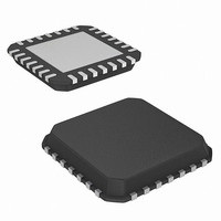
ISL6551IR-T Intersil, ISL6551IR-T Datasheet - Page 11

ISL6551IR-T
Manufacturer Part Number
ISL6551IR-T
Description
IC CTRL PWM ZVS FULL BRDG 28-QFN
Manufacturer
Intersil
Datasheet
1.ISL6551IBZ.pdf
(26 pages)
Specifications of ISL6551IR-T
Pwm Type
Current Mode
Number Of Outputs
6
Frequency - Max
1MHz
Duty Cycle
50%
Voltage - Supply
10.8 V ~ 13.2 V
Buck
No
Boost
No
Flyback
Yes
Inverting
No
Doubler
No
Divider
No
Cuk
No
Isolated
No
Operating Temperature
0°C ~ 85°C
Package / Case
28-VQFN Exposed Pad, 28-HVQFN, 28-SQFN, 28-DHVQFN
Frequency-max
1MHz
Lead Free Status / RoHS Status
Contains lead / RoHS non-compliant
- Note that the capacitance of a scope probe (~12pF for
- The dead time is the delay to turn on the upper FET
3,000
2,500
2,000
1,500
1,000
500
single ended) would induce a smaller frequency at the
CT pin. It can be easily seen at a higher frequency. An
accurate operating frequency can be measured at the
outputs of the bridge/synchronous drivers.
(UPPER1/UPPER2) after its corresponding lower FET
(LOWER1/LOWER2) is turned off when the bridge is
operating at maximum duty cycle in normal conditions,
or is responding to load transients or input line dipping
conditions. This helps to prevent shoot through between
the upper FET and the lower FET that are located at the
same side of the bridge. The dead time can be
estimated using Equation 2:
DT
where M=11.4(VDD=12V), 11.1(VDD=14V), and
12(VDD=10V), and RD is in kΩ. This relationship is
shown in Figure 3.
0
10
120°C
60°C
=
0°C
M
------------------- -
×
kΩ
RD
FIGURE 2. CT vs FREQUENCY
R
CSS
CSS
(ns)
RECOMMENDED RANGE
100
SHUTDOWN
11
CT (pF)
Iss
VDD
1,000
400mV
FIGURE 4. SIMPLIFIED CLAMP/SOFT-START
(EQ. 2)
+
-
10,000
ISL6551
(TO
BLANKING
CIRCUIT)
(See Fig. 9)
SSL
• Error Amplifier (EAI, EANI, EAO)
• Soft-Start (CSS)
- This amplifier compares the feedback signal received at
- Both EANI and EAO are clamped by the voltage
- The voltage on an external capacitor charged by an
- The clamping voltage determines the cycle-by-cycle
the EAI pin to a reference signal set at the EANI pin and
provides an error signal (EAO) to the PWM Logic. The
feedback loop compensation can be programmed via
these pins.
(Vclamp) set at the CSS pin, as shown in Figure 4. Note
that the diodes in the functional block diagram represent
the clamp function of the CSS in a simplified way.
internal current source I
the error amplifier. This causes the Error Amplifier to: 1)
limit the EAO to the soft-start voltage level; and 2) over-
ride the reference signal at the EANI with the soft-start
voltage, when the EANI voltage is higher than the soft-
start voltage. Thus, both the output voltage and current
of the power supply can be controlled by the soft-start.
peak current limiting of the power supply. It should be
set above the EANI and EAO voltages and can be
programmed by an external resistor as shown in
Figure 4 using Equation 3.
Vclamp
0.4
1.6
1.2
0.8
2
0
FIGURE 3. RD vs DEAD TIME (VDD = 12V)
ERROR AMP
0
=
Rcss
20
40
•
Iss
60
SS
RD (kΩ)
(V)
is fed into a control pin on
80
100
EAO
120
EAI
(–)
EANI
(+)
140
January 3, 2006
160
(EQ. 3)
FN9066.5


