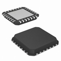
ISL6551IR-T Intersil, ISL6551IR-T Datasheet - Page 3

ISL6551IR-T
Manufacturer Part Number
ISL6551IR-T
Description
IC CTRL PWM ZVS FULL BRDG 28-QFN
Manufacturer
Intersil
Datasheet
1.ISL6551IBZ.pdf
(26 pages)
Specifications of ISL6551IR-T
Pwm Type
Current Mode
Number Of Outputs
6
Frequency - Max
1MHz
Duty Cycle
50%
Voltage - Supply
10.8 V ~ 13.2 V
Buck
No
Boost
No
Flyback
Yes
Inverting
No
Doubler
No
Divider
No
Cuk
No
Isolated
No
Operating Temperature
0°C ~ 85°C
Package / Case
28-VQFN Exposed Pad, 28-HVQFN, 28-SQFN, 28-DHVQFN
Frequency-max
1MHz
Lead Free Status / RoHS Status
Contains lead / RoHS non-compliant
Functional Pin Description
19, 20
21, 22
23, 24
26, 27
SOIC
PACKAGE PIN #
10
11
12
13
14
15
16
17
18
25
28
1
2
3
4
5
6
7
8
9
16, 17
18, 19
20, 21
23, 24
QFN
26
27
28
10
12
13
14
15
22
25
11
1
2
3
4
5
6
7
8
9
LOWER2, LOWER1
UPPER2, UPPER1
SYNC2, SYNC1
VDDP2, VDDP1
PIN SYMBOL
3
R_RESDLY
CS_COMP
ON/OFF
ISENSE
BGREF
SHARE
PKILIM
R_LEB
LATSD
DCOK
PGND
R_RA
EANI
CSS
EAO
VDD
VSS
EAI
CT
RD
Reference ground. All control circuits are referenced to this pin.
Set the oscillator frequency, up to 1MHz.
Adjust the clock dead time from 50ns to 1000ns.
Program the resonant delay from 50ns to 500ns.
Adjust the ramp for slope compensation (from 50mV to 250mV).
The pin receives the current information via a current sense transformer or a power resistor.
Set the over current limit with the bandgap reference as the trip threshold.
Precision bandgap reference, 1.263V ±2% overall recommended operating conditions.
Program the leading edge blanking from 50ns to 300ns.
Set a low current sharing loop bandwidth with a capacitor.
Program the rise time and the clamping voltage with a capacitor and a resistor, respectively.
Non-inverting input of Error Amp. It is clamped by the voltage at the CSS pin (Vclamp).
Inverting input of Error Amp. It receives the feedback voltage.
Output of Error Amp. It is clamped by the voltage at the CSS pin (Vclamp).
This pin is the SHARE BUS connecting with other unit(s) for current share operation.
The IC is latched off with a voltage greater than 3V at this pin and is reset by recycling VDD.
Power Good indication with a ±5% window.
This is an Enable pin that controls the states of all drive signals and the soft-start.
These are the gate control signals for the output synchronous rectifiers.
Both lower drivers are PWM-controlled on the trailing edge.
Both upper drivers are driven at a fixed 50% duty cycle.
Power Ground. High current return paths for both the upper and the lower drivers.
Power is delivered to both the upper and the lower drivers through these pins.
Power is delivered to all control circuits including SYNC1 & SYNC2 via this pin.
ISL6551
FUNCTION
January 3, 2006
FN9066.5


