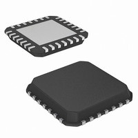
ISL6551IR-T Intersil, ISL6551IR-T Datasheet - Page 5

ISL6551IR-T
Manufacturer Part Number
ISL6551IR-T
Description
IC CTRL PWM ZVS FULL BRDG 28-QFN
Manufacturer
Intersil
Datasheet
1.ISL6551IBZ.pdf
(26 pages)
Specifications of ISL6551IR-T
Pwm Type
Current Mode
Number Of Outputs
6
Frequency - Max
1MHz
Duty Cycle
50%
Voltage - Supply
10.8 V ~ 13.2 V
Buck
No
Boost
No
Flyback
Yes
Inverting
No
Doubler
No
Divider
No
Cuk
No
Isolated
No
Operating Temperature
0°C ~ 85°C
Package / Case
28-VQFN Exposed Pad, 28-HVQFN, 28-SQFN, 28-DHVQFN
Frequency-max
1MHz
Lead Free Status / RoHS Status
Contains lead / RoHS non-compliant
Absolute Maximum Ratings
Supply Voltage VDD, VDDP1, VDDP2 . . . . . . . . . . . . . . -0.3 to 16V
Enable Inputs (ON/OFF, LATSD) . . . . . . . . . . . . . . . . . . . . . . . . VDD
Power Good Sink Current (I
ESD Rating
Recommended Operating Conditions
Ambient Temperature Range
ISL6551IB . . . . . . . . . . . . . . . . . . . . . . . . . . . . . . . . . . . 0°C to 85°C
ISL6551AB. . . . . . . . . . . . . . . . . . . . . . . . . . . . . . . . .-40°C to 105°C
Supply Voltage Range, VDD . . . . . . . . . . . . . . . . . . . 10.8V to 13.2V
Supply Voltage Range, VDDP1 & VDDP2 . . . . . . . . . . . . . . . <13.2V
Maximum Operating Junction Temperature . . . . . . . . . . . . . . . 125°C
CAUTION: Stresses above those listed in “Absolute Maximum Ratings” may cause permanent damage to the device. This is a stress only rating and operation of the
device at these or any other conditions above those indicated in the operational sections of this specification is not implied.
NOTES:
Electrical Specifications
SUPPLY (VDD, VDDP1, VDDP2)
Supply Voltage
Bias Current from VDD (ISL6551IB)
Bias Current from VDD (ISL6551AB)
Total Current from VDD and VDDP
UNDER VOLTAGE LOCKOUT (UVLO)
Start Threshold (ISL6551IB)
Start Threshold (ISL6551AB)
Stop Threshold (ISL6551IB)
Stop Threshold (ISL6551AB)
Hysteresis (ISL6551IB)
Hysteresis (ISL6551AB)
CLOCK GENERATOR (CT, RD)
Frequency Range
Dead Time Pulse Width (Note 4)
BANDGAP REFERENCE (BGREF)
Bandgap Reference Voltage
(ISL6551IB)
Bandgap Reference Voltage
(ISL6551AB)
Bandgap Reference Output Current
1. θ
2. θ
3. For θ
Human Body Model (Per MIL-STD-883 Method 3015.7) . . . . .3kV
Machine Model (Per EIAJ ED-4701 Method C-111) . . . . . . . .250V
Tech Brief TB379 for details.
JA
JA
is measured in free air with the component mounted on a high effective thermal conductivity test board with “direct attach” features. See
is measured with the component mounted on a high effective thermal conductivity test board in free air. See Tech Brief TB379 for details.
JC
, the “case temp” location is the center of the exposed metal pad on the package underside.
PARAMETER
DCOK
) . . . . . . . . . . . . . . . . . . . . . . 5mA
5
These specifications apply for VDD = VDDP = 12V and T
(ISL6551AB), Unless Otherwise Stated
SYMBOL
VDD
VDD
VDD
VDD
VDD
VDD
VREF
VREF
IREF
VDD
IDD
IDD
ICC
DT
F
OFF
OFF
HYS
HYS
ON
ON
VDD = 12V (not including drivers current at VDDP)
VDD = 12V (not including drivers current at VDDP)
VDD = VDDP = 12V, F = 1MHz, 1.6nF Load
VDD = 12V (Figure 2)
VDD = 12V (Figure 3)
VDD = 12V, 399kΩ pull-up, 0.1µF, after trimming
VDD = 12V, 399kΩ pull-up, 0.1µF, after trimming
VDD = 12V, see Block/Pin Functional Descriptions
for details
ISL6551
TEST CONDITIONS
Thermal Information
Thermal Resistance
Maximum Junction Temperature (Plastic Package) . . . . . . . . 150°C
Maximum Storage Temperature Range . . . . . . . . . . . -65°C to 150°C
Maximum Lead Temperature (Soldering 10s) . . . . . . . . . . . . . 300°C
QFN Package (Notes 1, 3). . . . . . . . . .
SOIC Package (Note 2) . . . . . . . . . . . .
(SOIC Lead Tips Only)
A
= 0°C to 85°C (ISL6551IB) or -40°C to 105°C
1.250
1.244
10.8
9.16
8.03
7.98
0.27
MIN
100
9.2
0.3
50
5
3
1.263
1.263
12.0
TYP
9.6
8.6
13
60
1
θ
JA
(°C/W)
30
55
1.280
1.287
MAX
1000
1000
13.2
9.94
8.87
8.92
1.93
100
9.9
1.9
18
20
January 3, 2006
θ
JC
UNITS
N/A
FN9066.5
2.5
(°C/W)
kHz
mA
mA
mA
µA
ns
V
V
V
V
V
V
V
V
V


