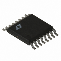
LT3837EFE#TRPBF Linear Technology, LT3837EFE#TRPBF Datasheet - Page 11

LT3837EFE#TRPBF
Manufacturer Part Number
LT3837EFE#TRPBF
Description
IC CNTRLR SYNC ISO 16TSSOP
Manufacturer
Linear Technology
Type
Flybackr
Datasheet
1.LT3837EFETRPBF.pdf
(28 pages)
Specifications of LT3837EFE#TRPBF
Internal Switch(s)
No
Synchronous Rectifier
Yes
Number Of Outputs
1
Frequency - Switching
50kHz ~ 250kHz
Voltage - Input
4.5 ~ 20 V
Operating Temperature
-40°C ~ 125°C
Mounting Type
Surface Mount
Package / Case
16-TSSOP Exposed Pad, 16-eTSSOP, 16-HTSSOP
Lead Free Status / RoHS Status
Lead free / RoHS Compliant
Current - Output
-
Voltage - Output
-
Power - Output
-
Available stocks
Company
Part Number
Manufacturer
Quantity
Price
OPERATION
Minimum Output Switch On-Time (t
The LT3837 affects output voltage regulation via fl yback
pulse action. If the output switch is not turned on, there
is no fl yback pulse and output voltage information is
not available. This causes irregular loop response and
start-up/latch-up problems. The solution is to require the
primary switch to be on for an absolute minimum time
per each oscillator cycle. If the output load is less than
that developed under these conditions, forced continuous
operation normally occurs. See the Applications Informa-
tion section for further details.
Enable Delay (ENDLY)
The fl yback pulse appears when the primary side switch
shuts off. However, it takes a fi nite time until the transformer
primary side voltage waveform represents the output
voltage. This is partly due to rise time on the primary
side MOSFET drain node but, more importantly, is due to
transformer leakage inductance. The latter causes a voltage
spike on the primary side, not directly related to output
voltage. Some time is also required for internal settling
of the feedback amplifi er circuitry. In order to maintain
immunity to these phenomena, a fi xed delay is introduced
between the switch turn-off command and the enabling of
the feedback amplifi er. This is termed “enable delay.” In
certain cases where the leakage spike is not suffi ciently
settled by the end of the enable delay period, regulation
error may result. See the Applications Information section
for further details.
Collapse Detect
Once the feedback amplifi er is enabled, some mechanism
is then required to disable it. This is accomplished by a
collapse detect comparator, which compares the fl yback
voltage (FB referred) to a fi xed reference, nominally 80%
of V
the feedback amplifi er is disabled.
Minimum Enable Time
The feedback amplifi er, once enabled, stays enabled for
a fi xed minimum time period termed “minimum enable
time.” This prevents lockup, especially when the output
voltage is abnormally low; e.g., during start-up. The mini-
FB
. When the fl yback waveform drops below this level,
ON(MIN)
)
mum enable time period ensures that the V
to pump up and increase the current mode trip point to
the level where the collapse detect system exhibits proper
operation. This time is internally set.
Effects of Variable Enable Period
The feedback amplifi er is enabled during only a portion of
the cycle time. This can vary from the fi xed minimum enable
time described to a maximum of roughly the “off” switch
time minus the enable delay time. Certain parameters of
fl yback amp behavior are directly affected by the variable
enable period. These include effective transconductance
and V
Load Compensation Theory
The LT3837 uses the fl yback pulse to obtain information
about the isolated output voltage. An error source is
caused by transformer secondary current fl ow through the
synchronous MOSFET R
ances of the transformer secondary and output capacitor.
This was represented previously by the expression “I
• (ESR + R
to convert this expression to effective output impedance.
Because the secondary current only fl ows during the off
portion of the duty cycle (DC), the effective output imped-
ance equals the lumped secondary impedance divided by
OFF time DC.
Since the OFF time duty cycle is equal to 1 – DC then:
where:
This impedance error may be judged acceptable in less
critical applications, or if the output load current remains
relatively constant. In these cases the external FB resistive
divider is adjusted to compensate for nominal expected
error. In more demanding applications, output impedance
error is minimized by the use of the load compensation
function.
R
DC = duty cycle
R
R
S(OUT)
DS(ON)
S OUT
C
(
node slew rate.
)
DS(ON)
= effective supply output impedance
and ESR are as defi ned previously
=
ESR R
).” However, it is generally more useful
1
+
–
DC
DS ON
DS(ON)
(
)
and real life nonzero imped-
LT3837
C
node is able
11
3837fc
SEC


