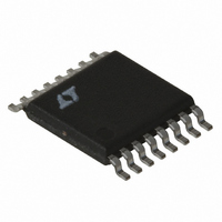
LT3837EFE#TRPBF Linear Technology, LT3837EFE#TRPBF Datasheet - Page 21

LT3837EFE#TRPBF
Manufacturer Part Number
LT3837EFE#TRPBF
Description
IC CNTRLR SYNC ISO 16TSSOP
Manufacturer
Linear Technology
Type
Flybackr
Datasheet
1.LT3837EFETRPBF.pdf
(28 pages)
Specifications of LT3837EFE#TRPBF
Internal Switch(s)
No
Synchronous Rectifier
Yes
Number Of Outputs
1
Frequency - Switching
50kHz ~ 250kHz
Voltage - Input
4.5 ~ 20 V
Operating Temperature
-40°C ~ 125°C
Mounting Type
Surface Mount
Package / Case
16-TSSOP Exposed Pad, 16-eTSSOP, 16-HTSSOP
Lead Free Status / RoHS Status
Lead free / RoHS Compliant
Current - Output
-
Voltage - Output
-
Power - Output
-
Available stocks
Company
Part Number
Manufacturer
Quantity
Price
APPLICATIONS INFORMATION
If the output load current is relatively constant, the feedback
resistive divider is used to compensate for these losses.
Otherwise, use the LT3837 load compensation circuitry
(see Load Compensation).
If multiple output windings are used, the fl yback winding
will have a signal that represents an amalgamation of all
these windings impedances. Take care that you examine
worst-case loading conditions when tweaking the volt-
ages.
Power MOSFET Selection
The power MOSFETs are selected primarily on the criteria of
on-resistance R
breakdown voltage (BV
and maximum drain current (I
For the primary-side power MOSFET, the peak current
is:
where X is peak-to-peak current ratio as defi ned earlier.
For each secondary-side power MOSFET, the peak cur-
rent is:
Select a primary-side power MOSFET with a B
than:
where N
mary winding. L
and C
C
may be added to reduce the leakage inductance spike as
discussed earlier.
For each secondary-side power MOSFET, the BV
be greater than:
OSS
BV
I
I
BV
PK
PK
DSS
DSS
P
of the primary-side power MOSFET). A snubber
=
=
is the primary-side capacitance (mostly from the
SP
1
1
≥ V
≥
–
–
refl ects the turns ratio of that secondary-to-pri-
I
I
I
DC
DC
OUT
OUT
PK
OUT
MAX
MAX
DS(ON)
LKG
L
+ V
C
LKG
is the primary-side leakage inductance
P
•
•
IN(MAX)
⎛
⎝ ⎜
⎛
⎝ ⎜
, input capacitance, drain-to-source
1
1
DSS
+
+
+
V
X
X
IN MAX
), maximum gate voltage (VGS)
MIN
MIN
2
2
(
• N
D(MAX)
⎞
⎠ ⎟
⎞
⎠ ⎟
SP
)
+
V
).
OUT MAX
N
SP
(
VDSS
)
DSS
greater
should
Choose the primary side MOSFET R
gate drive voltage (7.5V). The secondary side MOSFET
gate drive voltage depends on the gate drive method.
Primary side power MOSFET RMS current is given by:
For each secondary-side power MOSFET RMS current is
given by:
Calculate MOSFET power dissipation next. Because the
primary-side power MOSFET may operate at high V
transition power loss term is included for accuracy. C
is the most critical parameter in determining the transition
loss, but is not directly specifi ed on the data sheets.
C
on most MOSFET data sheets (Figure 6).
The fl at portion of the curve is the result of the Miller
(gate-to-drain) capacitance as the drain voltage drops.
The Miller capacitance is computed as:
The curve is done for a given V
for different V
computed C
the curve specifi ed V
MILLER
I
I
C
RMSPRI
RMSSEC
MILLER
is calculated from the gate charge curve included
=
=
=
MILLER
V
DS
Q
IN MIN
B
1–
Figure 6. Gate Charge Curve
(
V
V
voltages are estimated by multiplying the
GS
–
DS
I
OUT
DC
Q
by the ratio of the application V
P
)
A
DS
Q
IN
MAX
a
A
GATE CHARGE (Q
DC
.
MILLER EFFECT
MAX
DS
. The Miller capacitance
G
Q
b
)
B
DS(ON)
3825 F06
at the nominal
LT3837
21
MILLER
DS
DS
3837fc
, a
to


