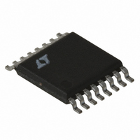
LT3837EFE#TRPBF Linear Technology, LT3837EFE#TRPBF Datasheet - Page 24

LT3837EFE#TRPBF
Manufacturer Part Number
LT3837EFE#TRPBF
Description
IC CNTRLR SYNC ISO 16TSSOP
Manufacturer
Linear Technology
Type
Flybackr
Datasheet
1.LT3837EFETRPBF.pdf
(28 pages)
Specifications of LT3837EFE#TRPBF
Internal Switch(s)
No
Synchronous Rectifier
Yes
Number Of Outputs
1
Frequency - Switching
50kHz ~ 250kHz
Voltage - Input
4.5 ~ 20 V
Operating Temperature
-40°C ~ 125°C
Mounting Type
Surface Mount
Package / Case
16-TSSOP Exposed Pad, 16-eTSSOP, 16-HTSSOP
Lead Free Status / RoHS Status
Lead free / RoHS Compliant
Current - Output
-
Voltage - Output
-
Power - Output
-
Available stocks
Company
Part Number
Manufacturer
Quantity
Price
APPLICATIONS INFORMATION
LT3837
IC Thermal Considerations
Take care to ensure that the LT3837 junction temperature
does not exceed 125°C. Power is computed from the aver-
age supply current, the sum of quiescent supply current
(I
The primary gate drive current is computed as:
where Q
the gate charge curve) and f is the switching frequency.
Since the synchronous driver is usually driving a capacitive
load, the power dissipation is:
where C
pin max voltage.
So total IC dissipation is computed as:
V
Junction temperature is computed as:
where:
PC Board Layout Considerations
In order to minimize switching noise and improve output
load regulation, connect the GND pin of the LT3837 directly
to the ground terminal of the V
the bottom terminal of the current sense resistor, the
ground terminal of the input capacitor, and the ground
plane (multiple vias). Place the V
adjacent to the V
24
CC
CC
f
f
P
T
T
θ
impedance (40°C/W).
OSC
OSC
A
J
JA
D(TOTAL)
is the worst-case LT3837 supply voltage.
in the specifi cations) plus gate drive currents.
= T
is the ambient temperature
is the FE16 package junction-to-ambient thermal
• Q
• C
G
S
A
is the total gate charge at max V
is the SG capacitive load and V
+ P
S
G
• V
= V
D
SGMAX
• θ
CC
CC
JA
• (I
and GND pins on the IC package.
CC
+ f •(Q
GPRI
CC
CC
capacitor immediately
decoupling capacitor,
+ C
GS
S
SGMAX
• V
(obtained from
SGMAX
is the SG
))
This capacitor carries high di/dt MOSFET gate drive cur-
rents. Use a low ESR ceramic capacitor.
Take care in PCB layout to keep the traces that conduct high
switching currents short, wide and with minimal overall
loop area. These are typically the traces associated with
the switches. This reduces the parasitic inductance and
also minimizes magnetic fi eld radiation. Figure 9 outlines
the critical paths.
Keep electric fi eld radiation low by minimizing the length
and area of traces (keep stray capacitances low). The drain
of the primary side MOSFET is the worst offender in this
category. Always use a ground plane under the switcher
circuitry to prevent coupling between PCB planes.
Check that the maximum BV
are not exceeded due to inductive ringing. This is done by
viewing the MOSFET node voltages with an oscilloscope. If
it is breaking down either choose a higher voltage device,
add a snubber or specify an avalanche-rated MOSFET.
Place the small-signal components away from high fre-
quency switching nodes. This allows the use of a pseudo-
Kelvin connection for the signal ground, where high di/dt
gate driver currents fl ow out of the IC ground pin in one
direction (to the bottom plate of the V
capacitor) and small-signal currents fl ow in the other
direction.
Keep the trace from the feedback divider tap to the FB
short to preclude inadvertent pickup.
For applications with multiple switching power converters
connected to the same input supply, make sure that the
input fi lter capacitor for the LTC3837 is not shared with
other converters. AC input current from another converter
could cause substantial input voltage ripple and this could
interfere with the LT3837 operation. A few inches of PC
trace or wire (L ≅ 100nH) between the C
and the actual source V
sharing problems.
IN
is suffi cient to prevent current
DSS
ratings of the MOSFETs
IN
CC
of the LT3837
decoupling
3837fc


