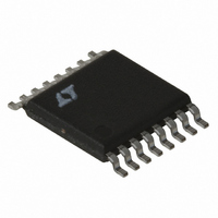
LT3837EFE#TRPBF Linear Technology, LT3837EFE#TRPBF Datasheet - Page 23

LT3837EFE#TRPBF
Manufacturer Part Number
LT3837EFE#TRPBF
Description
IC CNTRLR SYNC ISO 16TSSOP
Manufacturer
Linear Technology
Type
Flybackr
Datasheet
1.LT3837EFETRPBF.pdf
(28 pages)
Specifications of LT3837EFE#TRPBF
Internal Switch(s)
No
Synchronous Rectifier
Yes
Number Of Outputs
1
Frequency - Switching
50kHz ~ 250kHz
Voltage - Input
4.5 ~ 20 V
Operating Temperature
-40°C ~ 125°C
Mounting Type
Surface Mount
Package / Case
16-TSSOP Exposed Pad, 16-eTSSOP, 16-HTSSOP
Lead Free Status / RoHS Status
Lead free / RoHS Compliant
Current - Output
-
Voltage - Output
-
Power - Output
-
Available stocks
Company
Part Number
Manufacturer
Quantity
Price
APPLICATIONS INFORMATION
ESR and ESL along with bulk capacitance directly affect
the output voltage ripple. The waveforms for a typical
fl yback converter are illustrated in Figure 7.
The maximum acceptable ripple voltage (expressed as a
percentage of the output voltage) is used to establish a
starting point for the capacitor values. For the purpose
of simplicity we will choose 2% for the maximum output
ripple, divided equally between the ESR step and the
charging/discharging ΔV. This percentage ripple changes,
depending on the requirements of the application. You can
modify the following equations.
For a 1% contribution to the total ripple voltage, the ESR
of the output capacitor is determined by:
The other 1% is due to the bulk C component, so use:
In many applications the output capacitor is created from
multiple capacitors to achieve desired voltage ripple, reli-
ability and cost goals. For example, a low ESR ceramic
capacitor can minimize the ESR step, while an electrolytic
capacitor satisfi es the required bulk C.
ESR
C
RIPPLE WAVEFORM
OUTPUT VOLTAGE
OUT
COUT
Figure 7. Typical Flyback Converter Waveforms
SECONDARY
≥
CURRENT
CURRENT
PRIMARY
1% •
≤
1
% •
V
I
OUT
OUT
V
V
COUT
OUT
•
I
PRI
f
OSC
V
• –
ESR
(
I
1
OUT
DC
MAX
I
PRI
N
)
DUE TO ESL
RINGING
3825 F07
SwitcherCAD is a trademark of Linear Technology Corporation.
Continuing our example, the output capacitor needs:
These electrical characteristics require paralleling several
low ESR capacitors possibly of mixed type.
Most capacitor ripple current ratings are based on 2000
hour life. This makes it advisable to derate the capacitor
or to choose a capacitor rated at a higher temperature
than required.
One way to reduce cost and improve output ripple is to
use a simple LC fi lter. Figure 8 shows an example of the
fi lter.
The design of the fi lter is beyond the scope of this data
sheet. However, as a starting point, use these general
guide lines. Start with a C
solution. Make C1 1/4 of C
pole independent of C
implemented with multiple ceramic capacitors. Make L1
smaller than the output inductance of the transformer. In
general, a 0.1μH fi lter inductor is suffi cient. Add a small
ceramic capacitor (C
V
ond-Stage LC Filter Design,” Ridley, Switching Power
Magazine, July 2000, p8-10.
Circuit simulation is a way to optimize output capacitance
and fi lters, just make sure to include the component
parasitics. LTC SwitcherCAD™ is a terrifi c free circuit
simulation tool that is available at www.linear.com. Final
optimization of output ripple must be done on a dedicated
PC board. Parasitic inductance due to poor layout can
signifi cantly impact ripple. Refer to the PC Board Layout
section for more details.
OUT
ESR
C
OUT
. For those interested in more details refer to “Sec-
SECONDARY
COUT
≥
WINDING
1
FROM
% % • . •
≤
1
% •
3 3 200
10
3 3
A
C1
47μF
.
OUT2
0.1μH
3
L1
OUT
V
Figure 8
kHz
• –
OUT
) for high frequency noise on
. The smaller C1 may be best
(
10
OUT
1 52 4
=
1/4 the size of the nonfi lter
A
C
470μF
OUT
1515
to make the second fi lter
. %
μ
V
)
OUT
F
C
1μF
=
OUT2
1 6
3837 F08
.
LT3837
m
R
Ω
LOAD
23
3837fc


