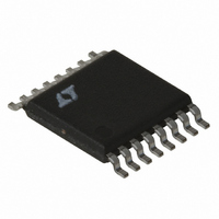
LT3837EFE#TRPBF Linear Technology, LT3837EFE#TRPBF Datasheet - Page 14

LT3837EFE#TRPBF
Manufacturer Part Number
LT3837EFE#TRPBF
Description
IC CNTRLR SYNC ISO 16TSSOP
Manufacturer
Linear Technology
Type
Flybackr
Datasheet
1.LT3837EFETRPBF.pdf
(28 pages)
Specifications of LT3837EFE#TRPBF
Internal Switch(s)
No
Synchronous Rectifier
Yes
Number Of Outputs
1
Frequency - Switching
50kHz ~ 250kHz
Voltage - Input
4.5 ~ 20 V
Operating Temperature
-40°C ~ 125°C
Mounting Type
Surface Mount
Package / Case
16-TSSOP Exposed Pad, 16-eTSSOP, 16-HTSSOP
Lead Free Status / RoHS Status
Lead free / RoHS Compliant
Current - Output
-
Voltage - Output
-
Power - Output
-
Available stocks
Company
Part Number
Manufacturer
Quantity
Price
APPLICATIONS INFORMATION
LT3837
ratio of between the two windings. Also keep the secondary
MOSFET R
Leakage Inductance
Transformer leakage inductance (on either the primary or
secondary) causes a spike after the primary side switch
turn-off. This is increasingly prominent at higher load
currents, where more stored energy is dissipated. Higher
fl yback voltage may break down the MOSFET switch if it
has too low a BV
One solution to reducing this spike is to use a snubber
circuit to suppress the voltage excursion. However, sup-
pressing the voltage extends the fl yback pulse width. If
the fl yback pulse extends beyond the enable delay time,
output voltage regulation is affected. The feedback system
has a deliberately limited input range, roughly ±50mV re-
ferred to the FB node. This rejects higher voltage leakage
spikes because once a leakage spike is several volts in
amplitude, a further increase in amplitude has little effect
on the feedback system.
So it is advisable to arrange the snubber circuit to clamp
at as high a voltage as possible, observing MOSFET
breakdown, such that leakage spike duration is as short
as possible. Application Note 19 provides a good reference
on snubber design.
As a rough guide, total leakage inductances of several per-
cent (of mutual inductance) or less may require a snubber,
but exhibit little to no regulation error due to leakage spike
behavior. Inductances from several percent up to perhaps
ten percent cause increasing regulation error.
Avoid double digit percentage leakage inductances as there
is a potential for abrupt loss of control at high load current.
This curious condition potentially occurs when the leakage
spike becomes such a large portion of the fl yback waveform
that the processing circuitry is fooled into thinking that the
leakage spike itself is the real fl yback signal!
It then reverts to a potentially stable state whereby the
top of the leakage spike is the control point, and the
trailing edge of the leakage spike triggers the collapse
detect circuitry. This typically reduces the output voltage
abruptly to a fraction, roughly one-third to two-thirds of
its correct value.
14
DS(ON)
DSS
small to improve cross regulation.
rating.
Once load current is reduced suffi ciently, the system snaps
back to normal operation. When using transformers with
considerable leakage inductance, exercise this worst-case
check for potential bistability:
1. Operate the prototype supply at maximum expected
2. Temporarily short-circuit the output.
3. Observe that normal operation is restored.
If the output voltage is found to hang up at an abnormally
low value, the system has a problem. This is usually evident
by simultaneously viewing the primary side MOSFET drain
voltage to observe fi rsthand the leakage spike behavior.
A fi nal note—the susceptibility of the system to bistable
behavior is somewhat a function of the load current/volt-
age characteristics. A load with resistive—i.e., I = V/R
behavior—is the most apt to be bistable. Capacitive loads
that exhibit I = V
Secondary Leakage Inductance
Leakage inductance on the secondary forms an inductive
divider on the transformer secondary, reducing the size
of the feedback fl yback pulse. This increases the output
voltage target by a similar percentage.
Note that unlike leakage spike behavior, this phenomenon
is independent of load. Since the secondary leakage in-
ductance is a constant percentage of mutual inductance
(within manufacturing variations), the solution is to adjust
the feedback resistive divider ratio to compensate.
Winding Resistance Effects
Primary or secondary winding resistance acts to reduce
overall effi ciency (P
increases effective output impedance degrading load regu-
lation. Load compensation can mitigate this to some extent
but a good design keeps parasitic resistances low.
Bifi lar Winding
A bifi lar or similar winding is a good way to minimize
troublesome leakage inductances. Bifi lar windings also
improve coupling coeffi cients and thus improve cross
regulation in multiple winding transformers. However,
load current.
2
/R behavior are less susceptible.
OUT
/P
IN
). Secondary winding resistance
3837fc


