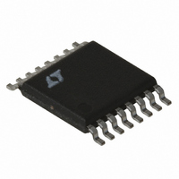
LT3837EFE#TRPBF Linear Technology, LT3837EFE#TRPBF Datasheet - Page 6

LT3837EFE#TRPBF
Manufacturer Part Number
LT3837EFE#TRPBF
Description
IC CNTRLR SYNC ISO 16TSSOP
Manufacturer
Linear Technology
Type
Flybackr
Datasheet
1.LT3837EFETRPBF.pdf
(28 pages)
Specifications of LT3837EFE#TRPBF
Internal Switch(s)
No
Synchronous Rectifier
Yes
Number Of Outputs
1
Frequency - Switching
50kHz ~ 250kHz
Voltage - Input
4.5 ~ 20 V
Operating Temperature
-40°C ~ 125°C
Mounting Type
Surface Mount
Package / Case
16-TSSOP Exposed Pad, 16-eTSSOP, 16-HTSSOP
Lead Free Status / RoHS Status
Lead free / RoHS Compliant
Current - Output
-
Voltage - Output
-
Power - Output
-
Available stocks
Company
Part Number
Manufacturer
Quantity
Price
LT3837
TYPICAL PERFORMANCE CHARACTERISTICS
PIN FUNCTIONS
SG (Pin 1): Synchronous gate drive output. This pin pro-
vides an output signal for a secondary-side synchronous
switch. Large dynamic currents may fl ow during voltage
transitions. See the Applications Information section for
details.
V
with a 4.7μF capacitor or more.
t
the minimum time that the primary switch is on for each
cycle. Minimum turn-on facilitates the isolated feedback
method. See the Applications Information section for
details.
ENDLY (Pin 4): Pin for external programming resistor to
set enable delay time. The enable delay time disables the
feedback amplifi er for a fi xed time after the turn-off of the
primary-side MOSFET. This allows the leakage inductance
voltage spike to be ignored for fl yback voltage sensing.
See the Applications Information section for details.
SYNC (Pin 5): Pin for synchronizing the internal oscillator
with an external clock. The positive edge on a pulse causes
the oscillator to discharge causing PG to go low (off) and
SG high (on). The sync threshold is typically 1.53V. See
the Applications Information section for details. Tie to
ground if unused.
6
ON
CC
(Pin 3): Pin for external programming resistor to set
(Pin 2): Supply voltage pin. Bypass this pin to ground
200
150
100
300
250
50
0
–50
PG Delay Time vs Temperature
–25
0
TEMPERATURE (°C)
R
R
25
PGDLY
PGDLY
50
= 27.4k
= 16.9k
75
100
3837 G19
125
SFST (Pin 6): This pin, in conjunction with a capacitor to
ground, controls the ramp-up of peak primary current as
sensed through the sense resistor. This is used to control
converter inrush current at start-up. The V
cannot exceed the SFST pin voltage, so as SFST increases,
the maximum voltage on V
allowing higher peak currents. Total V
proximately 70ms per μF of capacitance. Leave pin open
if not using the soft-start function.
OSC (Pin 7): This pin in conjunction with an external
capacitor defi nes the controller oscillator frequency. The
frequency is approximately 100kHz • 100/C
FB (Pin 8): Pin for the feedback node for the power supply
feedback amplifi er. Feedback is sensed via a transformer
winding and enabled during the fl yback period. This pin
also sinks additional current to compensate for load current
variation as set by the R
lent resistance of the feedback divider at roughly 3k.
260
240
180
140
220
200
160
–50
Enable Delay Time vs Temperature
R
ENDLY
–25
= 90k
0
TEMPERATURE (°C)
25
CMP
50
pin. Keep the Thevenin equiva-
C
75
increases commensurately,
100
3837 G20
125
C
ramp time is ap-
C
OSC
pin voltage
(pF).
3837fc


