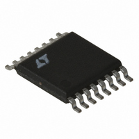
LT3837EFE#TRPBF Linear Technology, LT3837EFE#TRPBF Datasheet - Page 22

LT3837EFE#TRPBF
Manufacturer Part Number
LT3837EFE#TRPBF
Description
IC CNTRLR SYNC ISO 16TSSOP
Manufacturer
Linear Technology
Type
Flybackr
Datasheet
1.LT3837EFETRPBF.pdf
(28 pages)
Specifications of LT3837EFE#TRPBF
Internal Switch(s)
No
Synchronous Rectifier
Yes
Number Of Outputs
1
Frequency - Switching
50kHz ~ 250kHz
Voltage - Input
4.5 ~ 20 V
Operating Temperature
-40°C ~ 125°C
Mounting Type
Surface Mount
Package / Case
16-TSSOP Exposed Pad, 16-eTSSOP, 16-HTSSOP
Lead Free Status / RoHS Status
Lead free / RoHS Compliant
Current - Output
-
Voltage - Output
-
Power - Output
-
Available stocks
Company
Part Number
Manufacturer
Quantity
Price
LT3837
APPLICATIONS INFORMATION
With C
MOSFET power dissipation:
where:
(1 + δ) is generally given for a MOSFET in the form of a
normalized RDS(ON) vs temperature curve. If you don’t
have a curve, use δ = 0.005/°C as an estimate.
The secondary-side power MOSFETs typically operate
at substantially lower V
losses. The dissipation is calculated using:
With power dissipation known, the MOSFETs’ junction
temperatures are obtained from the equation:
where T
junction to ambient thermal resistance.
Once you have T
δ, power dissipations until convergence.
Gate Drive Node Consideration
The PG and SG gate drivers are strong drives to minimize
gate drive rise and fall times. This improves effi ciency
but the high frequency components of these signals can
cause problems. Keep the traces short and wide to reduce
parasitic inductance.
The parasitic inductance creates an LC tank with the
MOSFET gate capacitance. In less than ideal layouts, a
series resistance of 5Ω or more may help to dampen the
ringing at the expense of slightly slower rise and fall times
and effi ciency.
The LT3837 gate drives will clamp the max gate voltage to
roughly 7.4V, so you can safely use MOSFETs with max
V
22
GS
R
V
f
P
T
P
V
OSC
TH
J
D(SEC)
DPRI
IN MAX
DR
of 10V or larger.
= T
(
MILLER
is the MOSFET gate threshold voltage
is the gate driver resistance approximately 10Ω
A
is the operating frequency.
A
is the ambient temperature and θ
=
+ P
= I
I
)
RMS PRI
•
determined, calculate the primary-side power
RMS(SEC)
P
D
IN
(
DC
• θ
(
J
M M AX
, iterate your calculations recomputing
IN
JA
)
2
•
)
2
R
•
DS
• R
DS ON
R
DR
, so you can neglect transition
(
DS(ON)
•
)
V
(
1 δ
GATE MAX
(1 + δ)
+
C
)
(
MILLER
+
JA
)
–
is the MOSFET
V
TH
•
f
OSC
Synchronous Gate Drive
There are several different ways to drive the synchronous
gate MOSFET. Full converter isolation requires the synchro-
nous gate drive to be isolated. This is usually accomplished
by way of a pulse transformer. Usually the pulse driver is
used to drive a buffer on the secondary as shown in the
application on the front page of this data sheet.
However, other schemes are possible. There are gate drivers
and secondary side synchronous controllers available that
provide the buffer function as well as additional features.
Capacitor Selection
In a fl yback converter, the input and output current fl ows in
pulses, placing severe demands on the input and output fi lter
capacitors. The input and output fi lter capacitors are selected
based on RMS current ratings and ripple voltage.
Select an input capacitor with a ripple current rating
greater than:
Continuing the example:
Input capacitor series resistance (ESR) and inductance
(ESL) need to be small as they affect electromagnetic
interference suppression. In some instances, high ESR can
also produce stability problems because fl yback converters
exhibit a negative input resistance characteristic. Refer to
Application Note 19 for more information.
The output capacitor is sized to handle the ripple current
and to ensure acceptable output voltage ripple. The output
capacitor should have an RMS current rating greater than:
This is calculated for each output in a multiple winding
application.
I
I
Continuing the example: :
RMS
RMS
I
I
RMS
RMS
=
=
37 5
V
=
=
IN MIN
9
I
P
10
.
(
OUT
V
IN
W
A
)
1–
1 52 4
1 52 4
–
DC
52 4
– 1
–
52 4
DC
DC
. %
MAX
DC
. %
. %
MAX
MAX
. %
MAX
=
=
10 5
3 97
.
.
A
A
3837fc


