PCM18XK1 Microchip Technology, PCM18XK1 Datasheet - Page 135
PCM18XK1
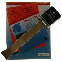
Manufacturer Part Number
PCM18XK1
Description
MODULE PROC PIC18F8680,6680,8565
Manufacturer
Microchip Technology
Datasheet
1.PCM18XK1.pdf
(496 pages)
Specifications of PCM18XK1
Accessory Type
Processor Module
Lead Free Status / RoHS Status
Not applicable / Not applicable
For Use With/related Products
ICE2000
For Use With
ICE2000 - EMULATOR MPLAB-ICE 2000 POD
Lead Free Status / Rohs Status
Lead free / RoHS Compliant


10.4
PORTD is an 8-bit wide, bidirectional port. The corre-
sponding data direction register is TRISD. Setting a
TRISD bit (= 1) will make the corresponding PORTD
pin an input (i.e., put the corresponding output driver in
a high-impedance mode). Clearing a TRISD bit (= 0)
will make the corresponding PORTD pin an output (i.e.,
put the contents of the output latch on the selected pin).
The Data Latch register (LATD) is also memory mapped.
Read-modify-write operations on the LATD register read
and write the latched output value for PORTD.
PORTD is an 8-bit port with Schmitt Trigger input
buffers. Each pin is individually configurable as an input
or output.
On PIC18F8X8X devices, PORTD is multiplexed with
the system bus as the external memory interface; I/O
port functions are only available when the system bus
is disabled by setting the EBDIS bit in the MEMCOM
register (MEMCON<7>). When operating as the exter-
nal memory interface, PORTD is the low-order byte of
the multiplexed address/data bus (AD7:AD0).
PORTD can also be configured as an 8-bit wide micro-
processor port (Parallel Slave Port) by setting control
bit, PSPMODE (TRISE<4>). In this mode, the input
buffers are TTL. See Section 10.10 “Parallel Slave
Port (PSP)” for additional information.
EXAMPLE 10-4:
2004 Microchip Technology Inc.
Note:
CLRF
CLRF
MOVLW
MOVWF
PORTD, TRISD and LATD
Registers
PORTD
LATD
0CFh
TRISD
On a Power-on Reset, these pins are
configured as digital inputs.
; Initialize PORTD by
; clearing output
; data latches
; Alternate method
; to clear output
; data latches
; Value used to
; initialize data
; direction
; Set RD<3:0> as inputs
; RD<5:4> as outputs
; RD<7:6> as inputs
INITIALIZING PORTD
PIC18F6585/8585/6680/8680
FIGURE 10-9:
RD TRISD
RD PORTD
RD LATD
Data
Bus
WR TRISD
Note 1:
WR LATD
or
PORTD
I/O pins have diode protection to V
TRIS Latch
Data Latch
D
D
CK
CK
PORTD BLOCK DIAGRAM
IN I/O PORT MODE
Q
Q
Q
EN
DS30491C-page 133
EN
Schmitt
Trigger
Input
Buffer
D
DD
and V
SS
I/O pin
.
(1)
Related parts for PCM18XK1
Image
Part Number
Description
Manufacturer
Datasheet
Request
R

Part Number:
Description:
Manufacturer:
Microchip Technology Inc.
Datasheet:
Part Number:
Description:
Manufacturer:
Microchip Technology Inc.
Datasheet:
Part Number:
Description:
Manufacturer:
Microchip Technology Inc.
Datasheet:
Part Number:
Description:
Manufacturer:
Microchip Technology Inc.
Datasheet:
Part Number:
Description:
Manufacturer:
Microchip Technology Inc.
Datasheet:
Part Number:
Description:
Manufacturer:
Microchip Technology Inc.
Datasheet:
Part Number:
Description:
Manufacturer:
Microchip Technology Inc.
Datasheet:
Part Number:
Description:
Manufacturer:
Microchip Technology Inc.
Datasheet: