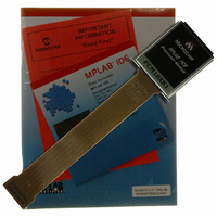
PCM18XK1 Microchip Technology, PCM18XK1 Datasheet - Page 257

PCM18XK1
Manufacturer Part Number
PCM18XK1
Description
MODULE PROC PIC18F8680,6680,8565
Manufacturer
Microchip Technology
Datasheet
1.PCM18XK1.pdf
(496 pages)
Specifications of PCM18XK1
Accessory Type
Processor Module
Lead Free Status / RoHS Status
Not applicable / Not applicable
For Use With/related Products
ICE2000
For Use With
ICE2000 - EMULATOR MPLAB-ICE 2000 POD
Lead Free Status / Rohs Status
Lead free / RoHS Compliant
- Current page: 257 of 496
- Download datasheet (9Mb)
19.3
The ADCON2 register allows the user to select an
acquisition time that occurs each time the GO/DONE
bit is set.
When the GO/DONE bit is set, sampling is stopped and
a conversion begins. The user is responsible for ensur-
ing the required acquisition time has passed between
selecting the desired input channel and setting the
GO/DONE bit. This occurs when the ACQT2:ACQT0
bits (ADCON2<5:3>) remain in their Reset state (‘000’)
and is compatible with devices that do not offer
programmable acquisition times.
If desired, the ACQT bits can be set to select a pro-
grammable acquisition time for the A/D module. When
the GO/DONE bit is set, the A/D module continues to
sample the input for the selected acquisition time, then
automatically begins a conversion. Since the acquisi-
tion time is programmed, there may be no need to wait
for an acquisition time between selecting a channel and
setting the GO/DONE bit.
In either case, when the conversion is completed, the
GO/DONE bit is cleared, the ADIF flag is set, and the
A/D begins sampling the currently selected channel
again. If an acquisition time is programmed, there is
nothing to indicate if the acquisition time has ended or
if the conversion has begun.
TABLE 19-1:
2004 Microchip Technology Inc.
Note 1:
2:
3:
Selecting and Configuring
Automatic Acquisition Time
Operation
The RC source has a typical T
The RC source has a typical T
For device frequencies above 1 MHz, the device must be in Sleep for the entire conversion or the A/D
accuracy may be out of specification.
16 T
32 T
64 T
2 T
4 T
8 T
RC
OSC
OSC
OSC
OSC
OSC
OSC
(3)
AD Clock Source (T
T
AD
vs. DEVICE OPERATING FREQUENCIES
ADCS2:ADCS0
AD
)
AD
AD
000
100
001
101
010
110
x11
time of 4 s.
time of 6 s.
PIC18F6585/8585/6680/8680
19.4
The A/D conversion time per bit is defined as T
A/D conversion requires 11 T
The source of the A/D conversion clock is software
selectable. There are seven possible options for T
For correct A/D conversions, the A/D conversion clock
(T
minimum T
for more information).
Table 19-1 shows the resultant T
the device operating frequencies and the A/D clock
source selected.
19.5
The ADCON1, TRISA, TRISF and TRISH registers con-
trol the operation of the A/D port pins. The port pins
needed as analog inputs must have their corresponding
TRIS bits set (input). If the TRIS bit is cleared (output),
the digital output level (V
The A/D operation is independent of the state of the
CHS3:CHS0 bits and the TRIS bits.
PIC18FXX80/XX85
AD
• 2 T
• 8 T
• 32 T
• Internal RC Oscillator
Note 1: When reading the port register, all pins
1.00 MHz
) must be as short as possible but greater than the
1.25 MHz
2.50 MHz
5.00 MHz
10.0 MHz
20.0 MHz
40.0 MHz
OSC
OSC
2: Analog levels on any pin defined as a dig-
Selecting the A/D Conversion Clock
Configuring Analog Port Pins
Maximum Device Frequency
OSC
AD
configured as analog input channels will
read as cleared (a low level). Pins config-
ured as digital inputs will convert an
analog input. Analog levels on a digitally
configured input will not affect the
conversion accuracy.
ital input may cause the input buffer to
consume current out of the device’s
specification limits.
(1)
(approximately 2 s, see parameter 130
OH
or V
AD
PIC18LFXX80/XX85
• 4 T
• 16 T
• 64 T
OL
per 10-bit conversion.
AD
) will be converted.
1.00 MHz
10.65 MHz
21.33 MHz
1.33 MHz
2.66 MHz
5.33 MHz
DS30491C-page 255
666 kHz
times derived from
OSC
OSC
OSC
(2)
AD
. The
AD
:
Related parts for PCM18XK1
Image
Part Number
Description
Manufacturer
Datasheet
Request
R

Part Number:
Description:
Manufacturer:
Microchip Technology Inc.
Datasheet:

Part Number:
Description:
Manufacturer:
Microchip Technology Inc.
Datasheet:

Part Number:
Description:
Manufacturer:
Microchip Technology Inc.
Datasheet:

Part Number:
Description:
Manufacturer:
Microchip Technology Inc.
Datasheet:

Part Number:
Description:
Manufacturer:
Microchip Technology Inc.
Datasheet:

Part Number:
Description:
Manufacturer:
Microchip Technology Inc.
Datasheet:

Part Number:
Description:
Manufacturer:
Microchip Technology Inc.
Datasheet:

Part Number:
Description:
Manufacturer:
Microchip Technology Inc.
Datasheet:


