PCM18XK1 Microchip Technology, PCM18XK1 Datasheet - Page 379
PCM18XK1
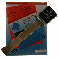
Manufacturer Part Number
PCM18XK1
Description
MODULE PROC PIC18F8680,6680,8565
Manufacturer
Microchip Technology
Datasheet
1.PCM18XK1.pdf
(496 pages)
Specifications of PCM18XK1
Accessory Type
Processor Module
Lead Free Status / RoHS Status
Not applicable / Not applicable
For Use With/related Products
ICE2000
For Use With
ICE2000 - EMULATOR MPLAB-ICE 2000 POD
Lead Free Status / Rohs Status
Lead free / RoHS Compliant


BRA
Syntax:
Operands:
Operation:
Status Affected:
Encoding:
Description:
Words:
Cycles:
Example:
2004 Microchip Technology Inc.
Q Cycle Activity:
Before Instruction
After Instruction
operation
Decode
PC
PC
No
Q1
Read literal
=
=
operation
Unconditional Branch
[ label ] BRA
-1024
(PC) + 2 + 2n
None
Add the 2’s complement number
‘2n’ to the PC. Since the PC will
have incremented to fetch the next
instruction, the new address will be
PC+2+2n. This instruction is a
two-cycle instruction.
1
2
HERE
1101
No
Q2
‘n’
address (HERE)
address (Jump)
n
0nnn
BRA
1023
operation
Process
Data
No
Q3
n
PC
Jump
nnnn
Write to PC
operation
PIC18F6585/8585/6680/8680
No
Q4
nnnn
BSF
Syntax:
Operands:
Operation:
Status Affected:
Encoding:
Description:
Words:
Cycles:
Example:
Q Cycle Activity:
Before Instruction
After Instruction
Decode
FLAG_REG
FLAG_REG
Q1
register ‘f’
Bit Set f
[ label ] BSF
0
0
a
1
None
Bit ‘b’ in register ‘f’ is set. If ‘a’ is ‘0’,
Access Bank will be selected, over-
riding the BSR value. If ‘a’ = 1, then
the bank will be selected as per the
BSR value.
1
1
BSF
Read
1000
Q2
=
=
f
b
[0,1]
f<b>
255
7
0x0A
0x8A
FLAG_REG, 7, 1
bbba
Process
Data
Q3
f,b[,a]
DS30491C-page 377
ffff
register ‘f’
Write
Q4
ffff
Related parts for PCM18XK1
Image
Part Number
Description
Manufacturer
Datasheet
Request
R

Part Number:
Description:
Manufacturer:
Microchip Technology Inc.
Datasheet:
Part Number:
Description:
Manufacturer:
Microchip Technology Inc.
Datasheet:
Part Number:
Description:
Manufacturer:
Microchip Technology Inc.
Datasheet:
Part Number:
Description:
Manufacturer:
Microchip Technology Inc.
Datasheet:
Part Number:
Description:
Manufacturer:
Microchip Technology Inc.
Datasheet:
Part Number:
Description:
Manufacturer:
Microchip Technology Inc.
Datasheet:
Part Number:
Description:
Manufacturer:
Microchip Technology Inc.
Datasheet:
Part Number:
Description:
Manufacturer:
Microchip Technology Inc.
Datasheet: