PCM18XK1 Microchip Technology, PCM18XK1 Datasheet - Page 202
PCM18XK1
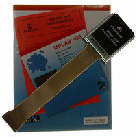
Manufacturer Part Number
PCM18XK1
Description
MODULE PROC PIC18F8680,6680,8565
Manufacturer
Microchip Technology
Datasheet
1.PCM18XK1.pdf
(496 pages)
Specifications of PCM18XK1
Accessory Type
Processor Module
Lead Free Status / RoHS Status
Not applicable / Not applicable
For Use With/related Products
ICE2000
For Use With
ICE2000 - EMULATOR MPLAB-ICE 2000 POD
Lead Free Status / Rohs Status
Lead free / RoHS Compliant


PIC18F6585/8585/6680/8680
REGISTER 17-4:
DS30491C-page 200
bit 7
bit 6
bit 5
bit 4
bit 3-0
SSPCON1: MSSP CONTROL REGISTER 1 (I
bit 7
WCOL: Write Collision Detect bit
In Master Transmit mode:
1 = A write to the SSPBUF register was attempted while the I
0 = No collision
In Slave Transmit mode:
1 = The SSPBUF register is written while it is still transmitting the previous word (must be
0 = No collision
In Receive mode (Master or Slave modes):
This is a “don’t care” bit.
SSPOV: Receive Overflow Indicator bit
In Receive mode:
1 = A byte is received while the SSPBUF register is still holding the previous byte (must be
0 = No overflow
In Transmit mode:
This is a “don’t care” bit in Transmit mode.
SSPEN: Synchronous Serial Port Enable bit
1 = Enables the serial port and configures the SDA and SCL pins as the serial port pins
0 = Disables serial port and configures these pins as I/O port pins
CKP: SCK Release Control bit
In Slave mode:
1 = Release clock
0 = Holds clock low (clock stretch), used to ensure data setup time
In Master mode:
Unused in this mode.
SSPM3:SSPM0: Synchronous Serial Port Mode Select bits
1111 = I
1110 = I
1011 = I
1000 = I
0111 = I
0110 = I
Legend:
R = Readable bit
- n = Value at POR
WCOL
R/W-0
Note:
Note:
a transmission to be started (must be cleared in software)
cleared in software)
cleared in software)
2
2
2
2
2
2
C Slave mode, 10-bit address with Start and Stop bit interrupts enabled
C Slave mode, 7-bit address with Start and Stop bit interrupts enabled
C Firmware Controlled Master mode (slave Idle)
C Master mode, clock = F
C Slave mode, 10-bit address
C Slave mode, 7-bit address
When enabled, the SDA and SCL pins must be properly configured as input or
output.
Bit combinations not specifically listed here are either reserved or implemented in
SPI mode only.
SSPOV
R/W-0
W = Writable bit
‘1’ = Bit is set
SSPEN
R/W-0
OSC
R/W-0
CKP
/(4 * (SSPADD + 1))
U = Unimplemented bit, read as ‘0’
‘0’ = Bit is cleared
SSPM3
R/W-0
2
C MODE)
SSPM2
R/W-0
2
C conditions were not valid for
2004 Microchip Technology Inc.
x = Bit is unknown
SSPM1
R/W-0
SSPM0
R/W-0
bit 0
Related parts for PCM18XK1
Image
Part Number
Description
Manufacturer
Datasheet
Request
R

Part Number:
Description:
Manufacturer:
Microchip Technology Inc.
Datasheet:
Part Number:
Description:
Manufacturer:
Microchip Technology Inc.
Datasheet:
Part Number:
Description:
Manufacturer:
Microchip Technology Inc.
Datasheet:
Part Number:
Description:
Manufacturer:
Microchip Technology Inc.
Datasheet:
Part Number:
Description:
Manufacturer:
Microchip Technology Inc.
Datasheet:
Part Number:
Description:
Manufacturer:
Microchip Technology Inc.
Datasheet:
Part Number:
Description:
Manufacturer:
Microchip Technology Inc.
Datasheet:
Part Number:
Description:
Manufacturer:
Microchip Technology Inc.
Datasheet: