PCM18XK1 Microchip Technology, PCM18XK1 Datasheet - Page 92
PCM18XK1
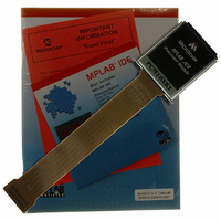
Manufacturer Part Number
PCM18XK1
Description
MODULE PROC PIC18F8680,6680,8565
Manufacturer
Microchip Technology
Datasheet
1.PCM18XK1.pdf
(496 pages)
Specifications of PCM18XK1
Accessory Type
Processor Module
Lead Free Status / RoHS Status
Not applicable / Not applicable
For Use With/related Products
ICE2000
For Use With
ICE2000 - EMULATOR MPLAB-ICE 2000 POD
Lead Free Status / Rohs Status
Lead free / RoHS Compliant


PIC18F6585/8585/6680/8680
5.5.1
The sequence of events for programming an internal
program memory location should be:
1.
2.
3.
4.
5.
6.
7.
EXAMPLE 5-3:
DS30491C-page 90
READ_BLOCK
MODIFY_WORD
Read 64 bytes into RAM.
Update data values in RAM as necessary.
Load table pointer with address being erased.
Do the row erase procedure.
Load table pointer with address of first byte
being written.
Write the first 8 bytes into the holding registers
with auto-increment.
Set the EECON1 register for the write operation:
• set EEPGD bit to point to program memory;
• clear the CFGS bit to access program memory;
• set WREN to enable byte writes.
FLASH PROGRAM MEMORY WRITE
SEQUENCE
MOVLW
MOVWF
MOVLW
MOVWF
MOVLW
MOVWF
MOVLW
MOVWF
MOVLW
MOVWF
MOVLW
MOVWF
TBLRD*+
MOVF
MOVWF
DECFSZ
BRA
MOVLW
MOVWF
MOVLW
MOVWF
MOVLW
MOVWF
MOVLW
MOVWF
WRITING TO FLASH PROGRAM MEMORY
D’64
COUNTER
high(BUFFER_ADDR)
FSR0H
low(BUFFER_ADDR)
FSR0L
upper(CODE_ADDR)
TBLPTRU
high(CODE_ADDR)
TBLPTRH
low(CODE_ADDR)
TBLPTRL
TABLAT, W
POSTINC0
COUNTER
READ_BLOCK
high(DATA_ADDR)
FSR0H
low(DATA_ADDR)
FSR0L
low(NEW_DATA)
POSTINC0
high(NEW_DATA)
INDF0
; number of bytes in erase block
; point to buffer
; Load TBLPTR with the base
; address of the memory block
; read into TABLAT, and inc
; get data
; store data
; done?
; repeat
; point to buffer
; update buffer word
8.
9.
10. Write 0AAh to EECON2.
11. Set the WR bit. This will begin the write cycle.
12. The CPU will stall for duration of the write (about
13. Execute a NOP.
14. Re-enable interrupts.
15. Repeat steps 6-14 seven times to write 64 bytes.
16. Verify the memory (table read).
This procedure will require about 40 ms to update one
row of 64 bytes of memory. An example of the required
code is given in Example 5-3.
Note:
Disable interrupts.
Write 55h to EECON2.
5 ms using internal timer).
Before setting the WR bit, the Table
Pointer address needs to be within the
intended address range of the eight bytes
in the holding register.
2004 Microchip Technology Inc.
Related parts for PCM18XK1
Image
Part Number
Description
Manufacturer
Datasheet
Request
R

Part Number:
Description:
Manufacturer:
Microchip Technology Inc.
Datasheet:
Part Number:
Description:
Manufacturer:
Microchip Technology Inc.
Datasheet:
Part Number:
Description:
Manufacturer:
Microchip Technology Inc.
Datasheet:
Part Number:
Description:
Manufacturer:
Microchip Technology Inc.
Datasheet:
Part Number:
Description:
Manufacturer:
Microchip Technology Inc.
Datasheet:
Part Number:
Description:
Manufacturer:
Microchip Technology Inc.
Datasheet:
Part Number:
Description:
Manufacturer:
Microchip Technology Inc.
Datasheet:
Part Number:
Description:
Manufacturer:
Microchip Technology Inc.
Datasheet: