PCM18XK1 Microchip Technology, PCM18XK1 Datasheet - Page 29
PCM18XK1
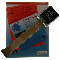
Manufacturer Part Number
PCM18XK1
Description
MODULE PROC PIC18F8680,6680,8565
Manufacturer
Microchip Technology
Datasheet
1.PCM18XK1.pdf
(496 pages)
Specifications of PCM18XK1
Accessory Type
Processor Module
Lead Free Status / RoHS Status
Not applicable / Not applicable
For Use With/related Products
ICE2000
For Use With
ICE2000 - EMULATOR MPLAB-ICE 2000 POD
Lead Free Status / Rohs Status
Lead free / RoHS Compliant


2.6.1
The system clock source switching is performed under
software control. The System Clock Switch bits,
SCS1:SCS0 (OSCCON<1:0>), control the clock switch-
ing. When the SCS0 bit is ‘0’, the system clock source
comes from the main oscillator that is selected by the
FOSC configuration bits in configuration register,
CONFIG1H. When the SCS0 bit is set, the system clock
source will come from the Timer1 oscillator. The SCS0
bit is cleared on all forms of Reset.
When FOSC bits are programmed for software PLL
mode, the SCS1 bit can be used to select between pri-
mary oscillator/clock and PLL output. The SCS1 bit will
only have an effect on the system clock if the PLL is
REGISTER 2-1:
2004 Microchip Technology Inc.
SYSTEM CLOCK SWITCH BIT
bit 7-4 Unimplemented: Read as ‘0’
bit 3
bit 2
bit 1
bit 0
OSCCON REGISTER
bit 7
LOCK: Phase Lock Loop Lock Status bit
1 = Phase Lock Loop output is stable as system clock
0 = Phase Lock Loop output is not stable and output cannot be used as system clock
PLLEN
1 = Enable Phase Lock Loop output as system clock
0 = Disable Phase Lock Loop
SCS1: System Clock Switch bit 1
When PLLEN and LOCK bits are set:
1 = Use PLL output
0 = Use primary oscillator/clock input pin
When PLLEN or LOCK bit is cleared:
Bit is forced clear.
SCS0
When OSCSEN configuration bit = 0 and T1OSCEN bit = 1:
1 = Switch to Timer1 oscillator/clock pin
0 = Use primary oscillator/clock input pin
When OSCSEN and T1OSCEN are in other states:
Bit is forced clear.
Legend:
R = Readable bit
- n = Value at POR
Note 1: PLLEN bit is ignored when configured for ECIO+PLL and HS+PLL. This bit is used
U-0
—
(2)
(1)
2: The setting of SCS0 = 1 supersedes SCS1 = 1.
: System Clock Switch bit 0
: Phase Lock Loop Enable bit
in ECIO+SPLL and HS+SPLL modes only.
U-0
—
PIC18F6585/8585/6680/8680
W = Writable bit
‘1’ = Bit is set
U-0
—
enabled (PLLEN = 1) and locked (LOCK = 1), else it will
be forced clear. When programmed with Configuration
Controlled PLL mode, the SCS1 bit will be forced clear.
U-0
—
Note:
U = Unimplemented bit, read as ‘0’
‘0’ = Bit is cleared
R/W-0
The Timer1 oscillator must be enabled
and operating to switch the system clock
source. The Timer1 oscillator is enabled
by setting the T1OSCEN bit in the Timer1
Control register (T1CON). If the Timer1
oscillator is not enabled, then any write to
the SCS0 bit will be ignored (SCS0 bit
forced cleared) and the main oscillator will
continue to be the system clock source.
LOCK
PLLEN
R/W-0
x = Bit is unknown
R/W-0
SCS1
DS30491C-page 27
R/W-0
SCS0
bit 0
Related parts for PCM18XK1
Image
Part Number
Description
Manufacturer
Datasheet
Request
R

Part Number:
Description:
Manufacturer:
Microchip Technology Inc.
Datasheet:
Part Number:
Description:
Manufacturer:
Microchip Technology Inc.
Datasheet:
Part Number:
Description:
Manufacturer:
Microchip Technology Inc.
Datasheet:
Part Number:
Description:
Manufacturer:
Microchip Technology Inc.
Datasheet:
Part Number:
Description:
Manufacturer:
Microchip Technology Inc.
Datasheet:
Part Number:
Description:
Manufacturer:
Microchip Technology Inc.
Datasheet:
Part Number:
Description:
Manufacturer:
Microchip Technology Inc.
Datasheet:
Part Number:
Description:
Manufacturer:
Microchip Technology Inc.
Datasheet: