ATEVK1105 Atmel, ATEVK1105 Datasheet - Page 385
ATEVK1105
Manufacturer Part Number
ATEVK1105
Description
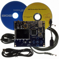
KIT EVAL FOR AT32UC3A0
Manufacturer
Atmel
Series
AVR®32r
Type
MCUr
Datasheets
1.ATAVRONE-PROBECBL.pdf
(16 pages)
2.ATEVK1104.pdf
(826 pages)
3.ATEVK1105.pdf
(28 pages)
Specifications of ATEVK1105
Contents
Evaluation Board, Software and Documentation
Processor To Be Evaluated
AT32UC3A0512
Processor Series
AVR
Data Bus Width
32 bit
Interface Type
USART, TWI, USB, SPI, Ethernet
Operating Supply Voltage
3.3 V
Silicon Manufacturer
Atmel
Core Architecture
AVR
Core Sub-architecture
AVR UC3
Silicon Core Number
AT32UC3A0512
Silicon Family Name
AVR
Kit Contents
Board CD Docs
Rohs Compliant
Yes
For Use With/related Products
AT32UC3A0
Lead Free Status / RoHS Status
Lead free / RoHS Compliant


27.6.5.2
32058J–AVR32–04/11
Early Read Wait State
In some cases, the SMC inserts a wait state cycle between a write access and a read access to
allow time for the write cycle to end before the subsequent read cycle begins. This wait state is
not generated in addition to a chip select wait state. The early read cycle thus only occurs
between a write and read access to the same memory device (same chip select).
• An early read wait state is automatically inserted if at least one of the following conditions is
• if the write controlling signal has no hold time and the read controlling signal has no setup time
• in NCS write controlled mode (WRITE_MODE = 0), if there is no hold timing on the NCS signal
• in NWE controlled mode (WRITE_MODE = 1) and if there is no hold timing (NWE_HOLD = 0),
Figure 27-18. Early Read Wait State: Write with No Hold Followed by Read with No Setup.
valid:
(Figure
and the NCS_RD_SETUP parameter is set to 0, regardless of the read mode
The write operation must end with a NCS rising edge. Without an Early Read Wait State, the
write operation could not complete properly.
the feedback of the write control signal is used to control address, data, chip select and byte
select lines. If the external write control signal is not inactivated as expected due to load
capacitances, an Early Read Wait State is inserted and address, data and control signals are
maintained one more cycle. See
NBS0, NBS1,
A0, A1
27-18).
CLK_SMC
A[25:2]
D[15:0]
NWE
NRD
Write cycle
Figure
No hold
27-20.
Early Read
Wait state
No setup
Read cycle
AT32UC3A
(Figure
27-19).
385
Related parts for ATEVK1105
Image
Part Number
Description
Manufacturer
Datasheet
Request
R

Part Number:
Description:
DEV KIT FOR AVR/AVR32
Manufacturer:
Atmel
Datasheet:

Part Number:
Description:
INTERVAL AND WIPE/WASH WIPER CONTROL IC WITH DELAY
Manufacturer:
ATMEL Corporation
Datasheet:
Part Number:
Description:
Low-Voltage Voice-Switched IC for Hands-Free Operation
Manufacturer:
ATMEL Corporation
Datasheet:
Part Number:
Description:
MONOLITHIC INTEGRATED FEATUREPHONE CIRCUIT
Manufacturer:
ATMEL Corporation
Datasheet:
Part Number:
Description:
AM-FM Receiver IC U4255BM-M
Manufacturer:
ATMEL Corporation
Datasheet:
Part Number:
Description:
Monolithic Integrated Feature Phone Circuit
Manufacturer:
ATMEL Corporation
Datasheet:
Part Number:
Description:
Multistandard Video-IF and Quasi Parallel Sound Processing
Manufacturer:
ATMEL Corporation
Datasheet:
Part Number:
Description:
High-performance EE PLD
Manufacturer:
ATMEL Corporation
Datasheet:
Part Number:
Description:
8-bit Flash Microcontroller
Manufacturer:
ATMEL Corporation
Datasheet:
Part Number:
Description:
2-Wire Serial EEPROM
Manufacturer:
ATMEL Corporation
Datasheet: