ATEVK1105 Atmel, ATEVK1105 Datasheet - Page 418
ATEVK1105
Manufacturer Part Number
ATEVK1105
Description
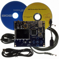
KIT EVAL FOR AT32UC3A0
Manufacturer
Atmel
Series
AVR®32r
Type
MCUr
Datasheets
1.ATAVRONE-PROBECBL.pdf
(16 pages)
2.ATEVK1104.pdf
(826 pages)
3.ATEVK1105.pdf
(28 pages)
Specifications of ATEVK1105
Contents
Evaluation Board, Software and Documentation
Processor To Be Evaluated
AT32UC3A0512
Processor Series
AVR
Data Bus Width
32 bit
Interface Type
USART, TWI, USB, SPI, Ethernet
Operating Supply Voltage
3.3 V
Silicon Manufacturer
Atmel
Core Architecture
AVR
Core Sub-architecture
AVR UC3
Silicon Core Number
AT32UC3A0512
Silicon Family Name
AVR
Kit Contents
Board CD Docs
Rohs Compliant
Yes
For Use With/related Products
AT32UC3A0
Lead Free Status / RoHS Status
Lead free / RoHS Compliant


Figure 28-6. Read Burst, 32-bit SDRAM Access
28.7.3
32058J–AVR32–04/11
SDRAMC_A[12:0]
Border Management
D[31:0]
SDWE
SDCS
(Input)
SDCK
RAS
CAS
For a single access or an incremented burst of unspecified length, the SDRAM Controller antici-
pates the next access. While the last value of the column is returned by the SDRAM Controller
on the bus, the SDRAM Controller anticipates the read to the next column and thus anticipates
the CAS latency. This reduces the effect of the CAS latency on the internal bus.
For burst access of specified length (4, 8, 16 words), access is not anticipated. This case leads
to the best performance. If the burst is broken (border, busy mode, etc.), the next access is han-
dled as an incrementing burst of unspecified length.
When the memory row boundary has been reached, an automatic page break is inserted. In this
case, the SDRAM controller generates a precharge command, activates the new row and initi-
ates a read or write command. To comply with SDRAM timing parameters, an additional clock
cycle is inserted between the precharge/active (t
mand. This is described in
Row n
t
RCD
= 3
col a
Figure 28-7
CAS = 2
col b
Dna
below.
col c
Dnb
col d
RP
) command and the active/read (t
Dnc
col e
Dnd
col f
Dne
Dnf
AT32UC3A
RCD
) com-
418
Related parts for ATEVK1105
Image
Part Number
Description
Manufacturer
Datasheet
Request
R

Part Number:
Description:
DEV KIT FOR AVR/AVR32
Manufacturer:
Atmel
Datasheet:

Part Number:
Description:
INTERVAL AND WIPE/WASH WIPER CONTROL IC WITH DELAY
Manufacturer:
ATMEL Corporation
Datasheet:
Part Number:
Description:
Low-Voltage Voice-Switched IC for Hands-Free Operation
Manufacturer:
ATMEL Corporation
Datasheet:
Part Number:
Description:
MONOLITHIC INTEGRATED FEATUREPHONE CIRCUIT
Manufacturer:
ATMEL Corporation
Datasheet:
Part Number:
Description:
AM-FM Receiver IC U4255BM-M
Manufacturer:
ATMEL Corporation
Datasheet:
Part Number:
Description:
Monolithic Integrated Feature Phone Circuit
Manufacturer:
ATMEL Corporation
Datasheet:
Part Number:
Description:
Multistandard Video-IF and Quasi Parallel Sound Processing
Manufacturer:
ATMEL Corporation
Datasheet:
Part Number:
Description:
High-performance EE PLD
Manufacturer:
ATMEL Corporation
Datasheet:
Part Number:
Description:
8-bit Flash Microcontroller
Manufacturer:
ATMEL Corporation
Datasheet:
Part Number:
Description:
2-Wire Serial EEPROM
Manufacturer:
ATMEL Corporation
Datasheet: