C8051F330DK Silicon Laboratories Inc, C8051F330DK Datasheet - Page 26
C8051F330DK
Manufacturer Part Number
C8051F330DK
Description
DEV KIT FOR C8051F330/F331
Manufacturer
Silicon Laboratories Inc
Type
MCUr
Specifications of C8051F330DK
Contents
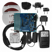
Evaluation Board, Power Supply, USB Cables, Adapter and Documentation
Processor To Be Evaluated
C8051F33x
Interface Type
RS-232
Operating Supply Voltage
7 V to 15 V
Silicon Manufacturer
Silicon Labs
Core Architecture
8051
Silicon Core Number
C8051F330
Silicon Family Name
C8051F33x
Lead Free Status / RoHS Status
Contains lead / RoHS non-compliant
For Use With/related Products
Silicon Laboratories C8051F330, C8051F331
Lead Free Status / Rohs Status
Lead free / RoHS Compliant
Other names
336-1264


C8051F330/1/2/3/4/5
1.7.
The C8051F330/2/4 devices include an on-chip 10-bit SAR ADC with a 16-channel differential input multi-
plexer. With a maximum throughput of 200 ksps, the ADC offers true 10-bit linearity with an INL and DNL of
±1 LSB. The ADC system includes a configurable analog multiplexer that selects both positive and nega-
tive ADC inputs. Ports0-1 are available as an ADC inputs; additionally, the on-chip Temperature Sensor
output and the power supply voltage (V
ADC to save power.
Conversions can be started in six ways: a software command, an overflow of Timer 0, 1, 2, or 3, or an
external convert start signal. This flexibility allows the start of conversion to be triggered by software
events, a periodic signal (timer overflows), or external HW signals. Conversion completions are indicated
by a status bit and an interrupt (if enabled). The resulting 10-bit data word is latched into the ADC data
SFRs upon completion of a conversion.
Window compare registers for the ADC data can be configured to interrupt the controller when ADC data is
either within or outside of a specified range. The ADC can monitor a key voltage continuously in back-
ground mode, but not interrupt the controller unless the converted data is within/outside the specified
range.
28
Sensor
Temp
VREF
GND
10-Bit Analog to Digital Converter
P0.0
P0.7
P1.0
P1.7
VDD
P0.0
P0.7
P1.0
P1.7
18-to-1
18-to-1
AMUX
AMUX
Figure 1.14. 10-Bit ADC Block Diagram
AMX0P
AMX0N
DD
) are available as ADC inputs. User firmware may shut down the
Rev. 1.7
(+)
(-)
ADC0CF
ADC
10-Bit
VDD
SAR
ADC0GTH ADC0GTL
ADC0LTH
ADC0CN
ADC0LTL
Conversion
Start
000
001
010
011
100
101
32
AD0WINT
Compare
Window
AD0BUSY (W)
Timer 0 Overflow
Timer 2 Overflow
Timer 1 Overflow
CNVSTR Input
Timer 3 Overflow
Logic
Related parts for C8051F330DK
Image
Part Number
Description
Manufacturer
Datasheet
Request
R

Part Number:
Description:
SMD/C°/SINGLE-ENDED OUTPUT SILICON OSCILLATOR
Manufacturer:
Silicon Laboratories Inc
Part Number:
Description:
Manufacturer:
Silicon Laboratories Inc
Datasheet:
Part Number:
Description:
N/A N/A/SI4010 AES KEYFOB DEMO WITH LCD RX
Manufacturer:
Silicon Laboratories Inc
Datasheet:
Part Number:
Description:
N/A N/A/SI4010 SIMPLIFIED KEY FOB DEMO WITH LED RX
Manufacturer:
Silicon Laboratories Inc
Datasheet:
Part Number:
Description:
N/A/-40 TO 85 OC/EZLINK MODULE; F930/4432 HIGH BAND (REV E/B1)
Manufacturer:
Silicon Laboratories Inc
Part Number:
Description:
EZLink Module; F930/4432 Low Band (rev e/B1)
Manufacturer:
Silicon Laboratories Inc
Part Number:
Description:
I°/4460 10 DBM RADIO TEST CARD 434 MHZ
Manufacturer:
Silicon Laboratories Inc
Part Number:
Description:
I°/4461 14 DBM RADIO TEST CARD 868 MHZ
Manufacturer:
Silicon Laboratories Inc
Part Number:
Description:
I°/4463 20 DBM RFSWITCH RADIO TEST CARD 460 MHZ
Manufacturer:
Silicon Laboratories Inc
Part Number:
Description:
I°/4463 20 DBM RADIO TEST CARD 868 MHZ
Manufacturer:
Silicon Laboratories Inc
Part Number:
Description:
I°/4463 27 DBM RADIO TEST CARD 868 MHZ
Manufacturer:
Silicon Laboratories Inc
Part Number:
Description:
I°/4463 SKYWORKS 30 DBM RADIO TEST CARD 915 MHZ
Manufacturer:
Silicon Laboratories Inc
Part Number:
Description:
N/A N/A/-40 TO 85 OC/4463 RFMD 30 DBM RADIO TEST CARD 915 MHZ
Manufacturer:
Silicon Laboratories Inc
Part Number:
Description:
I°/4463 20 DBM RADIO TEST CARD 169 MHZ
Manufacturer:
Silicon Laboratories Inc