C8051F330DK Silicon Laboratories Inc, C8051F330DK Datasheet - Page 8
C8051F330DK
Manufacturer Part Number
C8051F330DK
Description
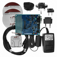
DEV KIT FOR C8051F330/F331
Manufacturer
Silicon Laboratories Inc
Type
MCUr
Specifications of C8051F330DK
Contents
Evaluation Board, Power Supply, USB Cables, Adapter and Documentation
Processor To Be Evaluated
C8051F33x
Interface Type
RS-232
Operating Supply Voltage
7 V to 15 V
Silicon Manufacturer
Silicon Labs
Core Architecture
8051
Silicon Core Number
C8051F330
Silicon Family Name
C8051F33x
Lead Free Status / RoHS Status
Contains lead / RoHS non-compliant
For Use With/related Products
Silicon Laboratories C8051F330, C8051F331
Lead Free Status / Rohs Status
Lead free / RoHS Compliant
Other names
336-1264


C8051F330/1/2/3/4/5
11. Flash Memory
12. External RAM
13. Oscillators
14. Port Input/Output
15. SMBus
16. UART0
17. Enhanced Serial Peripheral Interface (SPI0)
18. Timers
8
Figure 10.2. Power-On and VDD Monitor Reset Timing .......................................... 98
Figure 11.1. Flash Program Memory Map.............................................................. 105
Figure 13.1. Oscillator Diagram.............................................................................. 113
Figure 13.2. External 32.768 kHz Quartz Crystal Oscillator Connection Diagram . 119
Figure 14.1. Port I/O Functional Block Diagram ..................................................... 123
Figure 14.2. Port I/O Cell Block Diagram ............................................................... 124
Figure 14.3. Crossbar Priority Decoder with No Pins Skipped ............................... 125
Figure 14.4. Crossbar Priority Decoder with Crystal Pins Skipped ........................ 126
Figure 15.1. SMBus Block Diagram ....................................................................... 135
Figure 15.2. Typical SMBus Configuration ............................................................. 136
Figure 15.3. SMBus Transaction ............................................................................ 137
Figure 15.4. Typical SMBus SCL Generation......................................................... 141
Figure 15.5. Typical Master Transmitter Sequence................................................ 147
Figure 15.6. Typical Master Receiver Sequence.................................................... 148
Figure 15.7. Typical Slave Receiver Sequence...................................................... 149
Figure 15.8. Typical Slave Transmitter Sequence.................................................. 150
Figure 16.1. UART0 Block Diagram ....................................................................... 153
Figure 16.2. UART0 Baud Rate Logic .................................................................... 154
Figure 16.3. UART Interconnect Diagram .............................................................. 155
Figure 16.4. 8-Bit UART Timing Diagram............................................................... 155
Figure 16.5. 9-Bit UART Timing Diagram............................................................... 156
Figure 16.6. UART Multi-Processor Mode Interconnect Diagram .......................... 157
Figure 17.1. SPI Block Diagram ............................................................................. 163
Figure 17.2. Multiple-Master Mode Connection Diagram ....................................... 166
Figure 17.3. 3-Wire Single Master and 3-Wire Single Slave Mode
Figure 17.4. 4-Wire Single Master Mode and 4-Wire Slave Mode
Figure 17.5. Master Mode Data/Clock Timing ........................................................ 168
Figure 17.6. Slave Mode Data/Clock Timing (CKPHA = 0) .................................... 169
Figure 17.7. Slave Mode Data/Clock Timing (CKPHA = 1) .................................... 169
Figure 17.8. SPI Master Timing (CKPHA = 0)........................................................ 173
Figure 17.9. SPI Master Timing (CKPHA = 1)........................................................ 173
Figure 17.10. SPI Slave Timing (CKPHA = 0)........................................................ 174
Figure 17.11. SPI Slave Timing (CKPHA = 1)........................................................ 174
Figure 18.1. T0 Mode 0 Block Diagram.................................................................. 178
Figure 18.2. T0 Mode 2 Block Diagram.................................................................. 179
Connection Diagram166
Connection Diagram166
Rev. 1.7
Related parts for C8051F330DK
Image
Part Number
Description
Manufacturer
Datasheet
Request
R

Part Number:
Description:
SMD/C°/SINGLE-ENDED OUTPUT SILICON OSCILLATOR
Manufacturer:
Silicon Laboratories Inc
Part Number:
Description:
Manufacturer:
Silicon Laboratories Inc
Datasheet:
Part Number:
Description:
N/A N/A/SI4010 AES KEYFOB DEMO WITH LCD RX
Manufacturer:
Silicon Laboratories Inc
Datasheet:
Part Number:
Description:
N/A N/A/SI4010 SIMPLIFIED KEY FOB DEMO WITH LED RX
Manufacturer:
Silicon Laboratories Inc
Datasheet:
Part Number:
Description:
N/A/-40 TO 85 OC/EZLINK MODULE; F930/4432 HIGH BAND (REV E/B1)
Manufacturer:
Silicon Laboratories Inc
Part Number:
Description:
EZLink Module; F930/4432 Low Band (rev e/B1)
Manufacturer:
Silicon Laboratories Inc
Part Number:
Description:
I°/4460 10 DBM RADIO TEST CARD 434 MHZ
Manufacturer:
Silicon Laboratories Inc
Part Number:
Description:
I°/4461 14 DBM RADIO TEST CARD 868 MHZ
Manufacturer:
Silicon Laboratories Inc
Part Number:
Description:
I°/4463 20 DBM RFSWITCH RADIO TEST CARD 460 MHZ
Manufacturer:
Silicon Laboratories Inc
Part Number:
Description:
I°/4463 20 DBM RADIO TEST CARD 868 MHZ
Manufacturer:
Silicon Laboratories Inc
Part Number:
Description:
I°/4463 27 DBM RADIO TEST CARD 868 MHZ
Manufacturer:
Silicon Laboratories Inc
Part Number:
Description:
I°/4463 SKYWORKS 30 DBM RADIO TEST CARD 915 MHZ
Manufacturer:
Silicon Laboratories Inc
Part Number:
Description:
N/A N/A/-40 TO 85 OC/4463 RFMD 30 DBM RADIO TEST CARD 915 MHZ
Manufacturer:
Silicon Laboratories Inc
Part Number:
Description:
I°/4463 20 DBM RADIO TEST CARD 169 MHZ
Manufacturer:
Silicon Laboratories Inc