MPC8349E-MITXE Freescale Semiconductor, MPC8349E-MITXE Datasheet - Page 28
MPC8349E-MITXE
Manufacturer Part Number
MPC8349E-MITXE
Description
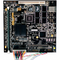
BOARD REFERENCE FOR MPC8349
Manufacturer
Freescale Semiconductor
Series
PowerQUICC II™ PROr
Type
MPUr
Specifications of MPC8349E-MITXE
Contents
Module and Misc Hardware
Processor To Be Evaluated
MPC8349E
Interface Type
Ethernet, USB
Silicon Manufacturer
Freescale
Core Architecture
Power Architecture
Core Sub-architecture
PowerQUICC
Silicon Core Number
MPC83xx
Silicon Family Name
PowerQUICC II PRO
Rohs Compliant
Yes
For Use With/related Products
MPC8349E
Lead Free Status / RoHS Status
Lead free / RoHS Compliant
Other names
MPC8349E-MITXE


MPC8349E-mITXE Board
Table 13
28
Position
C
D
G
H
A
B
E
F
describes the position of each jumper.
PCI_M66EN
I2C-WP
BOOT1
LGPL0
LGPL1
LGPL3
LGPL5
Name
F_WP
OFF = Jumper Is Off
ON = Jumper Is On
MPC8349E-mITXE Reference Design Platform User’s Guide, Rev. 2
OFF (1)
OFF (1)
Default
ON (0)
ON (0)
ON (0)
ON (0)
ON (0)
ON (0)
Table 13. Description of Jumper J22 Positions
Preliminary—Subject to Change Without Notice
000 local bus EEPROM (Default)
001 I
010 I
011 Hard-coded option, 66 MHz, 266 MHz, 400 MHz (PCI, CSB, CPU)
100 Hard-coded option, 33 MHz, 266 MHz, 400 MHz
101 Hard-coded option, 33 MHz, 133 MHz, 266 MHz
110 Hard-coded option, 33 MHz, 166 MHz, 333 MHz
111 Hard-coded option, 66 MHz, 266 MHz, 533 MHz
Hard-coded option is used in conjunction with JTAG debug
OFF (1): Default
CLKIN: PCI_SYNC_OUT = 2:1 PCI_CLK_OUT[0:7] = OCCR (max CLKIN/2).
Use if 66 MHz CLKIN is used with 66 MHz PCI1 and 33 MHz PCI2.
ON (0):
CLKIN: PCI_SYNC_OUT = 1:1, PCI_CLK_OUT[0:7] = CLKIN. Use if the
PCI1 and PCI2 have the same frequency and the PCI frequency = CLKIN.
OFF (1):
MPC8349E fetches the reset vector from Flash 0 (U4).
ON (0): Default
MPC8349E fetches the reset vector from Flash 1 (U7).
OFF (1):
M66EN signal is determined by the card plugged into the PCI slot (PCI 32-bit
slot and MiniPCI slot).
ON (0): Default
M66EN signal is hardwired to 0, which is hard coded to 33 MHz PCI
operation.
OFF (1):
I
ON (0): Default
I
OFF (1): Default
Flash (U4 and U7) are not write protected.
ON (0):
Flash (U4 and U7) are write protected.
2
2
C EEPROM (U64) is write protected.
C EEPROM (U64) is not write protected.
2
2
C EEPROM,PCI_CLK/PCI_SYNC_IN 25–44 MHz
C EEPROM,PCI_CLK/PCI_SYNC_IN 25–66.666 MHz
Description
Freescale Semiconductor
Related parts for MPC8349E-MITXE
Image
Part Number
Description
Manufacturer
Datasheet
Request
R

Part Number:
Description:
KIT REFERENCE PLATFORM MPC8349E
Manufacturer:
Freescale Semiconductor
Datasheet:
Part Number:
Description:
KIT MODULAR DEV SYSTEM MPC8349E
Manufacturer:
Freescale Semiconductor
Datasheet:

Part Number:
Description:
MCU, MPU & DSP Development Tools PROCESSR BD MPC8349E
Manufacturer:
Freescale Semiconductor
Part Number:
Description:
MCU, MPU & DSP Development Tools KIT FOR MPC8349E BDS
Manufacturer:
Freescale Semiconductor

Part Number:
Description:
Manufacturer:
Freescale Semiconductor, Inc
Datasheet:
Part Number:
Description:
Manufacturer:
Freescale Semiconductor, Inc
Datasheet:
Part Number:
Description:
Manufacturer:
Freescale Semiconductor, Inc
Datasheet:
Part Number:
Description:
Manufacturer:
Freescale Semiconductor, Inc
Datasheet:
Part Number:
Description:
Manufacturer:
Freescale Semiconductor, Inc
Datasheet:
Part Number:
Description:
Manufacturer:
Freescale Semiconductor, Inc
Datasheet:
Part Number:
Description:
Manufacturer:
Freescale Semiconductor, Inc
Datasheet:
Part Number:
Description:
Manufacturer:
Freescale Semiconductor, Inc
Datasheet:
Part Number:
Description:
Manufacturer:
Freescale Semiconductor, Inc
Datasheet:
Part Number:
Description:
Manufacturer:
Freescale Semiconductor, Inc
Datasheet:
Part Number:
Description:
Manufacturer:
Freescale Semiconductor, Inc
Datasheet: