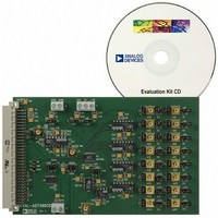
EVAL-AD7490CB Analog Devices Inc, EVAL-AD7490CB Datasheet - Page 16
EVAL-AD7490CB
Manufacturer Part Number
EVAL-AD7490CB
Description
BOARD EVAL FOR AD7490
Manufacturer
Analog Devices Inc
Datasheet
1.AD7490BRUZ.pdf
(28 pages)
Specifications of EVAL-AD7490CB
Number Of Adc's
1
Number Of Bits
12
Sampling Rate (per Second)
1M
Data Interface
Serial
Inputs Per Adc
16 Single Ended
Input Range
0 ~ 5 V
Power (typ) @ Conditions
12.5mW @ 1MSPS, 5 V
Voltage Supply Source
Single
Operating Temperature
-40°C ~ 85°C
Utilized Ic / Part
AD7490
Lead Free Status / RoHS Status
Contains lead / RoHS non-compliant


AD7490
THEORY OF OPERATION
CIRCUIT INFORMATION
The AD7490 is a fast, 16-channel, 12-bit, single-supply, analog-
to-digital converter. The parts can be operated from a 2.7 V to
5.25 V supply. When operated from a 5 V supply and provided
with a 20 MHz clock, the AD7490 is capable of throughput rates
of up to 1 MSPS.
The AD7490 provides the user with an on-chip, track-and-hold
ADC and a serial interface housed in either a 28-lead TSSOP or
32-lead LFCSP package. The AD7490 has 16 single-ended input
channels with a channel sequencer, allowing the user to select a
sequence of channels through which the ADC can cycle with each
consecutive CS falling edge. The serial clock input accesses data
from the part, controls the transfer of data written to the ADC,
and provides the clock source for the successive approximation
ADC. The analog input range for the AD74790 is 0 V to REF
or 0 V to 2 × REF
control register. For the 0 V to 2 × REF
operated from a 4.75 V to 5.25 V supply.
The AD7490 provides flexible power management options to
allow the user to achieve the best power performance for a
given throughput rate. These options are selected by program-
ming the power management bits in the control register.
CONVERTER OPERATION
The AD7490 is a 12-bit successive approximation ADC based
around a capacitive DAC. The AD7490 can convert analog
input signals in the range 0 V to REF
Figure 15 and Figure 16 show simplified schematics of the
ADC. The ADC comprises control logic, SAR, and a capacitive
DAC, which are used to add and subtract fixed amounts of
charge from the sampling capacitor to bring the comparator
back into a balanced condition. Figure 15 shows the ADC
during its acquisition phase. SW2 is closed and SW1 is in
Position A. The comparator is held in a balanced condition,
and the sampling capacitor acquires the signal on the selected
V
When the ADC starts a conversion (see Figure 16), SW2 opens
and SW1 moves to Position B, causing the comparator to become
unbalanced. The control logic and the capacitive DAC are used
to add and subtract fixed amounts of charge from the sampling
capacitor to bring the comparator back into a balanced condi-
tion. When the comparator is rebalanced, the conversion is
complete. The control logic generates the ADC output code.
Figure 18 shows the ADC transfer function.
IN
channel.
IN
, depending on the status of Bit 1 in the
IN
IN
or 0 V to 2 × REF
range, the part must be
IN
.
Rev. C | Page 16 of 28
IN
Analog Input
Figure 17 shows an equivalent circuit of the analog input struc-
ture of the AD7490. The two diodes, D1 and D2, provide ESD
protection for the analog inputs. Care must be taken to ensure
that the analog input signal never exceeds the supply rails by
more than 200 mV. This causes these diodes to become forward
biased and to start conducting current into the substrate. The
maximum current these diodes can conduct without causing
irreversible damage to the part is 10 mA. Capacitor C1 in Figure 17
is typically about 4 pF and can primarily be attributed to pin
capacitance. Resistor R1 is a lumped component made up of the
on resistance of a track-and-hold switch and includes the on
resistance of the input multiplexer. The total resistance is typically
about 400 Ω. Capacitor C2 is the ADC sampling capacitor and
typically has a capacitance of 30 pF.
For ac applications, removing high frequency components from
the analog input signal is recommended by use of an RC low-
pass filter on the relevant analog input pin. In applications where
harmonic distortion and signal-to-noise ratio are critical, the
analog input should be driven from a low impedance source.
Large source impedances significantly affect the ac performance
of the ADC. This may necessitate the use of an input buffer
amplifier. The choice of the op amp is a function of the particular
application.
AGND
AGND
V
V
V
V
IN
IN
IN
IN
15
15
0
0
V
IN
4pF
Figure 17. Equivalent Analog Input Circuit
C1
SW1
SW1
Figure 15. ADC Acquisition Phase
Figure 16. ADC Conversion Phase
A
A
CONVERSION PHASE—SWITCH OPEN
TRACK PHASE—SWITCH CLOSED
D1
D2
B
B
V
DD
4kΩ
4kΩ
SW2
SW2
R1
COMPARATOR
COMPARATOR
30pF
C2
CAPACITIVE
CAPACITIVE
CONTROL
CONTROL
LOGIC
LOGIC
DAC
DAC
Related parts for EVAL-AD7490CB
Image
Part Number
Description
Manufacturer
Datasheet
Request
R

Part Number:
Description:
ENERCHIP CC EVAL KIT
Manufacturer:
Cymbet Corporation
Datasheet:

Part Number:
Description:
BOARD EVAL FOR AD976
Manufacturer:
Analog Devices Inc
Datasheet:

Part Number:
Description:
BOARD EVAL FOR ADXL345
Manufacturer:
Analog Devices Inc
Datasheet:

Part Number:
Description:
ENERCHIP CC SEH EVAL KIT
Manufacturer:
Cymbet Corporation
Datasheet:

Part Number:
Description:
ENERCHIP EP ENERGY HARVEST EVAL
Manufacturer:
Cymbet Corporation
Datasheet:

Part Number:
Description:
EVAL BOARD FOR TW6864-LB2-GR
Manufacturer:
Intersil
Datasheet:
Part Number:
Description:
EVAL BOARD FOR TW8816-LB3-GR
Manufacturer:
Intersil
Datasheet:
Part Number:
Description:
EVAL BOARD FOR TW8817-TA3-GRS
Manufacturer:
Intersil
Datasheet:

Part Number:
Description:
EVALUATION MODULE FOR ADUM4160
Manufacturer:
Analog Devices Inc
Datasheet:

Part Number:
Description:
BOARD EVALUATION ADCMP581BCP
Manufacturer:
Analog Devices Inc
Datasheet:
Part Number:
Description:
BOARD EVALUATION ADM1041
Manufacturer:
Analog Devices Inc
Datasheet:

Part Number:
Description:
EVAL BOARD FOR STM32F107VCT
Manufacturer:
STMicroelectronics
Datasheet:
Part Number:
Description:
BOARD EVAL FOR AD1954
Manufacturer:
Analog Devices Inc
Datasheet:
Part Number:
Description:
BOARD EVAL FOR AD1955
Manufacturer:
Analog Devices Inc
Datasheet:

Part Number:
Description:
BOARD EVAL FOR AD7655
Manufacturer:
Analog Devices Inc
Datasheet: