EVAL-AD7490CB Analog Devices Inc, EVAL-AD7490CB Datasheet - Page 25
EVAL-AD7490CB
Manufacturer Part Number
EVAL-AD7490CB
Description
BOARD EVAL FOR AD7490
Manufacturer
Analog Devices Inc
Datasheet
1.AD7490BRUZ.pdf
(28 pages)
Specifications of EVAL-AD7490CB
Number Of Adc's
1
Number Of Bits
12
Sampling Rate (per Second)
1M
Data Interface
Serial
Inputs Per Adc
16 Single Ended
Input Range
0 ~ 5 V
Power (typ) @ Conditions
12.5mW @ 1MSPS, 5 V
Voltage Supply Source
Single
Operating Temperature
-40°C ~ 85°C
Utilized Ic / Part
AD7490
Lead Free Status / RoHS Status
Contains lead / RoHS non-compliant


Set the word length to 16 by setting WL1 = 1 and WL0 = 0 in
CRA. The FSP bit in the CRB should be set to 1 so the frame
sync is negative. Note that for signal processing applications, it
is imperative that the frame synchronization signal from the
DSP563xx provide equidistant sampling.
In the example shown in Figure 32, the serial clock is taken
from the ESSI so the SCK0 pin must be set as an output, SCKD
= 1. The AD7490 V
that of the DSP563xx. This allows the ADC to operate at a
higher voltage than the serial interface, that is, DSP563xx, if
necessary.
APPLICATION HINTS
Grounding and Layout
The AD7490 has very good immunity to noise on the power
supplies shown in the PSRR vs. Supply Ripple Frequency plot,
Figure 7. Care should still be taken, however, with regard to
grounding and layout.
The printed circuit board that houses the AD7490 should be
designed such that the analog and digital sections are separated
and confined to certain areas of the board. This facilitates the
use of ground planes that can be separated easily. A minimum
etch technique is generally best for ground planes because it
gives the best shielding. All three AGND pins of the AD7490
should be sunk in the AGND plane. Digital and analog ground
planes should be joined at only one place. If the AD7490 is in a
system where multiple devices require an AGND to DGND
connection, the connection should still be made at one point
only, a star ground point that should be established as close as
possible to the AD7490.
Avoid running digital lines under the device because these
couple noise onto the die. The analog ground plane should be
allowed to run under the AD7490 to avoid noise coupling. The
power supply lines to the AD7490 should use as large a trace as
possible to provide low impedance paths and reduce the effects
of glitches on the power supply line. Fast switching signals like
clocks should be shielded with digital ground to avoid radiating
noise to other sections of the board, and clock signals should
never be run near the analog inputs. Avoid crossover of digital
*ADDITIONAL PINS REMOVED FOR CLARITY
AD7490
Figure 32. Interfacing to the DSP563xx
V
SCLK
DOUT
DRIVE
DIN
DRIVE
CS
pin takes the same supply voltage as
SCK
SRD
STD
SC2
DSP563xx*
V
DD
Rev. C | Page 25 of 28
and analog signals. Traces on opposite sides of the board should
run at right angles to each other. This reduces the effects of
feedthrough through the board. A microstrip technique is by far
the best but is not always possible with a double-sided board. In
this technique, the component side of the board is dedicated to
ground planes, and signals are placed on the solder side.
Good decoupling is also important. All analog supplies should
be decoupled with 10 μF tantalum in parallel with 0.1 μF capaci-
tors to AGND. To achieve the best from these decoupling
components, they must be placed as close as possible to the
device, ideally right up against the device. The 0.1 μF capacitors
should have low effective series resistance (ESR) and effective
series inductance (ESI), such as the common ceramic types or
surface mount types, which provide a low impedance path to
ground at high frequencies to handle transient currents due to
internal logic switching.
PCB Design Guidelines for Chip Scale Package
The lands on the chip scale package (CP-32) are rectangular.
The printed circuit board pad for these should be 0.1 mm
longer than the package land length and 0.05 mm wider than
the package land width. The land should be centered on the
pad. This ensures that the solder joint size is maximized. The
bottom of the chip scale package has a central thermal pad. The
thermal pad on the printed circuit board should be at least as
large as this exposed pad. On the printed circuit board, there
should be a clearance of at least 0.25 mm between the thermal
pad and the inner edges of the pad pattern. This ensures that
shorting is avoided. Thermal vias can be used on the printed
circuit board thermal pad to improve thermal performance of
the package. If vias are used, they should be incorporated in the
thermal pad at 1.2 mm pitch grid. The via diameter should be
between 0.3 mm and 0.33 mm, and the via barrel should be
plated with 1 oz. copper to plug the via. The user should
connect the printed circuit board thermal pad to AGND.
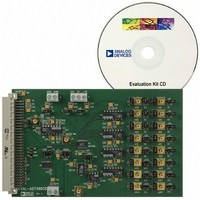
Evaluating the AD7490 Performance
The recommended layout for the AD7490 is outlined in the
evaluation board for the AD7490. The evaluation board package
includes a fully assembled and tested evaluation board, documen-
tation, and software for controlling the board from the PC via
the EVAL-CONTROL BRD2. The EVAL-CONTROL BRD2 can
be used in conjunction with the AD7490 evaluation board, as
well as many other Analog Devices, Inc., evaluation boards
ending in the CB designator, to demonstrate and evaluate the ac
and dc performance of the AD7490.
The software allows the user to perform ac (fast Fourier
transform) and dc (histogram of codes) tests on the AD7490.
The software and documentation are on a CD shipped with the
evaluation board.
AD7490
Related parts for EVAL-AD7490CB
Image
Part Number
Description
Manufacturer
Datasheet
Request
R

Part Number:
Description:
ENERCHIP CC EVAL KIT
Manufacturer:
Cymbet Corporation
Datasheet:

Part Number:
Description:
BOARD EVAL FOR AD976
Manufacturer:
Analog Devices Inc
Datasheet:

Part Number:
Description:
BOARD EVAL FOR ADXL345
Manufacturer:
Analog Devices Inc
Datasheet:

Part Number:
Description:
ENERCHIP CC SEH EVAL KIT
Manufacturer:
Cymbet Corporation
Datasheet:

Part Number:
Description:
ENERCHIP EP ENERGY HARVEST EVAL
Manufacturer:
Cymbet Corporation
Datasheet:

Part Number:
Description:
EVAL BOARD FOR TW6864-LB2-GR
Manufacturer:
Intersil
Datasheet:
Part Number:
Description:
EVAL BOARD FOR TW8816-LB3-GR
Manufacturer:
Intersil
Datasheet:
Part Number:
Description:
EVAL BOARD FOR TW8817-TA3-GRS
Manufacturer:
Intersil
Datasheet:

Part Number:
Description:
EVALUATION MODULE FOR ADUM4160
Manufacturer:
Analog Devices Inc
Datasheet:

Part Number:
Description:
BOARD EVALUATION ADCMP581BCP
Manufacturer:
Analog Devices Inc
Datasheet:
Part Number:
Description:
BOARD EVALUATION ADM1041
Manufacturer:
Analog Devices Inc
Datasheet:

Part Number:
Description:
EVAL BOARD FOR STM32F107VCT
Manufacturer:
STMicroelectronics
Datasheet:
Part Number:
Description:
BOARD EVAL FOR AD1954
Manufacturer:
Analog Devices Inc
Datasheet:
Part Number:
Description:
BOARD EVAL FOR AD1955
Manufacturer:
Analog Devices Inc
Datasheet:

Part Number:
Description:
BOARD EVAL FOR AD7655
Manufacturer:
Analog Devices Inc
Datasheet: