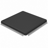
LPC2388FBD144,551 NXP Semiconductors, LPC2388FBD144,551 Datasheet - Page 12

LPC2388FBD144,551
Manufacturer Part Number
LPC2388FBD144,551
Description
IC ARM7 MCU FLASH 512K 144LQFP
Manufacturer
NXP Semiconductors
Series
LPC2300r
Specifications of LPC2388FBD144,551
Program Memory Type
FLASH
Program Memory Size
512KB (512K x 8)
Package / Case
144-LQFP
Core Processor
ARM7
Core Size
16/32-Bit
Speed
72MHz
Connectivity
CAN, EBI/EMI, Ethernet, I²C, Microwire, MMC, SPI, SSI, SSP, UART/USART, USB OTG
Peripherals
Brown-out Detect/Reset, DMA, I²S, POR, PWM, WDT
Number Of I /o
104
Ram Size
98K x 8
Voltage - Supply (vcc/vdd)
3 V ~ 3.6 V
Data Converters
A/D 8x10b; D/A 1x10b
Oscillator Type
Internal
Operating Temperature
-40°C ~ 85°C
Processor Series
LPC23
Core
ARM7TDMI-S
Data Bus Width
16 bit, 32 bit
Data Ram Size
98 KB
Interface Type
CAN/I2C/I2S/SPI/SSP/UART/USB
Maximum Clock Frequency
72 MHz
Number Of Programmable I/os
104
Number Of Timers
4
Operating Supply Voltage
3.3 V
Maximum Operating Temperature
+ 85 C
Mounting Style
SMD/SMT
3rd Party Development Tools
MDK-ARM, RL-ARM, ULINK2, MCB2388, MCB2388U, MCB2388UME
Development Tools By Supplier
OM11012
Minimum Operating Temperature
- 40 C
On-chip Adc
8-ch x 10-bit
On-chip Dac
1-ch x 10-bit
Lead Free Status / RoHS Status
Lead free / RoHS Compliant
For Use With
OM11012 - BOARD EVAL FOR LPC2388568-3999 - BOARD EVAL FOR LPC23 ARM MCU622-1005 - USB IN-CIRCUIT PROG ARM7 LPC2K
Eeprom Size
-
Lead Free Status / Rohs Status
Lead free / RoHS Compliant
Other names
568-4323
935285417551
LPC2388FBD144-S
935285417551
LPC2388FBD144-S
Available stocks
Company
Part Number
Manufacturer
Quantity
Price
Company:
Part Number:
LPC2388FBD144,551
Manufacturer:
NXP Semiconductors
Quantity:
10 000
NXP Semiconductors
Table 3.
LPC2388_0
Preliminary data sheet
Symbol
P2[11]/EINT1/
MCIDAT1/
I2STX_CLK
P2[12]/EINT2/
MCIDAT2/
I2STX_WS
P2[13]/EINT3/
MCIDAT3/
I2STX_SDA
P3[0] to P3[31]
P3[0]/D0
P3[1]/D1
P3[2]/D2
P3[3]/D3
P3[4]/D4
P3[5]/D5
P3[6]/D6
P3[7]/D7
P3[23]/CAP0[0]/
PCAP1[0]
P3[24]/CAP0[1]/
PWM1[1]
Pin description
Pin
75
73
71
137
140
144
2
9
12
16
19
45
40
[1]
[1]
[6]
[6]
[6]
[1]
[1]
[1]
[1]
[1]
[1]
[1]
[1]
…continued
Type
I/O
I
O
I/O
I/O
I
O
I/O
I/O
I
O
I/O
I/O
I/O
I/O
I/O
I/O
I/O
I/O
I/O
I/O
I/O
I/O
I/O
I/O
I/O
I/O
I/O
I/O
I/O
I
I
I/O
I
O
Description
P2[11] — General purpose digital input/output pin.
EINT1 — External interrupt 1 input.
MCIDAT1 — Data line for SD/MMC interface.
I2STX_CLK — Transmit Clock. It is driven by the master and received by the slave.
Corresponds to the signal SCK in the I
P2[12] — General purpose digital input/output pin.
EINT2 — External interrupt 2 input.
MCIDAT2 — Data line for SD/MMC interface.
I2STX_WS — Transmit Word Select. It is driven by the master and received by the
slave. Corresponds to the signal WS in the I
P2[13] — General purpose digital input/output pin.
EINT3 — External interrupt 3 input.
MCIDAT3 — Data line for SD/MMC interface.
I2STX_SDA — Transmit data. It is driven by the transmitter and read by the
receiver. Corresponds to the signal SD in the I
Port 3: Port 3 is a 32 bit I/O port with individual direction controls for each bit. The
operation of port 3 pins depends upon the pin function selected via the Pin Connect
block. Pins 8 through 22, and 27 through 31 of this port are not available.
P3[0] — General purpose digital input/output pin.
D0 — External memory data line 0.
P3[1] — General purpose digital input/output pin.
D1 — External memory data line 1.
P3[2] — General purpose digital input/output pin.
D2 — External memory data line 2.
P3[3] — General purpose digital input/output pin.
D3 — External memory data line 3.
P3[4] — General purpose digital input/output pin.
D4 — External memory data line 4.
P3[5] — General purpose digital input/output pin.
D5 — External memory data line 5.
P3[6] — General purpose digital input/output pin.
D6 — External memory data line 6.
P3[7] — General purpose digital input/output pin.
D7 — External memory data line 7.
P3[23] — General purpose digital input/output pin.
CAP0[0] — Capture input for Timer 0, channel 0.
PCAP1[0] — Capture input for PWM1, channel 0.
P3[24] — General purpose digital input/output pin.
CAP0[1] — Capture input for Timer 0, channel 1.
PWM1[1] — Pulse Width Modulator 1, output 1.
Rev. 00.01 — 23 October 2007
2
S-bus specification.
2
S-bus specification.
2
S-bus specification.
Fast communication chip
LPC2388
© NXP B.V. 2007. All rights reserved.
12 of 57


