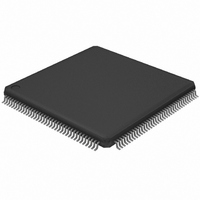
LPC2388FBD144,551 NXP Semiconductors, LPC2388FBD144,551 Datasheet - Page 31

LPC2388FBD144,551
Manufacturer Part Number
LPC2388FBD144,551
Description
IC ARM7 MCU FLASH 512K 144LQFP
Manufacturer
NXP Semiconductors
Series
LPC2300r
Specifications of LPC2388FBD144,551
Program Memory Type
FLASH
Program Memory Size
512KB (512K x 8)
Package / Case
144-LQFP
Core Processor
ARM7
Core Size
16/32-Bit
Speed
72MHz
Connectivity
CAN, EBI/EMI, Ethernet, I²C, Microwire, MMC, SPI, SSI, SSP, UART/USART, USB OTG
Peripherals
Brown-out Detect/Reset, DMA, I²S, POR, PWM, WDT
Number Of I /o
104
Ram Size
98K x 8
Voltage - Supply (vcc/vdd)
3 V ~ 3.6 V
Data Converters
A/D 8x10b; D/A 1x10b
Oscillator Type
Internal
Operating Temperature
-40°C ~ 85°C
Processor Series
LPC23
Core
ARM7TDMI-S
Data Bus Width
16 bit, 32 bit
Data Ram Size
98 KB
Interface Type
CAN/I2C/I2S/SPI/SSP/UART/USB
Maximum Clock Frequency
72 MHz
Number Of Programmable I/os
104
Number Of Timers
4
Operating Supply Voltage
3.3 V
Maximum Operating Temperature
+ 85 C
Mounting Style
SMD/SMT
3rd Party Development Tools
MDK-ARM, RL-ARM, ULINK2, MCB2388, MCB2388U, MCB2388UME
Development Tools By Supplier
OM11012
Minimum Operating Temperature
- 40 C
On-chip Adc
8-ch x 10-bit
On-chip Dac
1-ch x 10-bit
Lead Free Status / RoHS Status
Lead free / RoHS Compliant
For Use With
OM11012 - BOARD EVAL FOR LPC2388568-3999 - BOARD EVAL FOR LPC23 ARM MCU622-1005 - USB IN-CIRCUIT PROG ARM7 LPC2K
Eeprom Size
-
Lead Free Status / Rohs Status
Lead free / RoHS Compliant
Other names
568-4323
935285417551
LPC2388FBD144-S
935285417551
LPC2388FBD144-S
Available stocks
Company
Part Number
Manufacturer
Quantity
Price
Company:
Part Number:
LPC2388FBD144,551
Manufacturer:
NXP Semiconductors
Quantity:
10 000
NXP Semiconductors
LPC2388_0
Preliminary data sheet
7.25.1.1 Internal RC oscillator
7.25.1.2 Main oscillator
7.25.1.3 RTC oscillator
7.25.1 Crystal oscillators
7.25.2 PLL
7.25 Clocking and power control
The LPC2388 includes three independent oscillators. These are the Main Oscillator, the
Internal RC oscillator, and the RTC oscillator. Each oscillator can be used for more than
one purpose as required in a particular application. Any of the three clock sources can be
chosen by software to drive the PLL and ultimately the CPU.
Following reset, the LPC2388 will operate from the Internal RC oscillator until switched by
software. This allows systems to operate without any external crystal and the bootloader
code to operate at a known frequency.
The IRC may be used as the clock source for the WDT, and/or as the clock that drives the
PLL and subsequently the CPU. The nominal IRC frequency is 4 MHz. The IRC is
trimmed to 1 % accuracy.
Upon power-up or any chip reset, the LPC2388 uses the IRC as the clock source.
Software may later switch to one of the other available clock sources.
The main oscillator can be used as the clock source for the CPU, with or without using the
PLL. The main oscillator operates at frequencies of 1 MHz to 24 MHz. This frequency can
be boosted to a higher frequency, up to the maximum CPU operating frequency, by the
PLL. The clock selected as the PLL input is PLLCLKIN. The ARM processor clock
frequency is referred to as CCLK elsewhere in this document. The frequencies of
PLLCLKIN and CCLK are the same value unless the PLL is active and connected. The
clock frequency for each peripheral can be selected individually and is referred to as
PCLK. Refer to
The RTC oscillator can be used as the clock source for the RTC and/or the WDT. Also, the
RTC oscillator can be used to drive the PLL and the CPU.
The PLL accepts an input clock frequency in the range of 32 kHz to 50 MHz. The input
frequency is multiplied up to a high frequency, then divided down to provide the actual
clock used by the CPU and the USB block.
The PLL input, in the range of 32 kHz to 50 MHz, may initially be divided down by a value
‘N’, which may be in the range of 1 to 256. This input division provides a wide range of
output frequencies from the same input frequency.
•
•
•
•
An alarm output pin is included to assist in waking up from Power-down mode, or
when the chip has had power removed to all functions except the RTC and Battery
RAM.
Periodic interrupts can be generated from increments of any field of the time registers,
and selected fractional second values.
2 kB data SRAM powered by VBAT.
RTC and Battery RAM power supply is isolated from the rest of the chip.
Section 7.25.2
Rev. 00.01 — 23 October 2007
for additional information.
Fast communication chip
LPC2388
© NXP B.V. 2007. All rights reserved.
31 of 57


