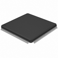
LPC2388FBD144,551 NXP Semiconductors, LPC2388FBD144,551 Datasheet - Page 33

LPC2388FBD144,551
Manufacturer Part Number
LPC2388FBD144,551
Description
IC ARM7 MCU FLASH 512K 144LQFP
Manufacturer
NXP Semiconductors
Series
LPC2300r
Specifications of LPC2388FBD144,551
Program Memory Type
FLASH
Program Memory Size
512KB (512K x 8)
Package / Case
144-LQFP
Core Processor
ARM7
Core Size
16/32-Bit
Speed
72MHz
Connectivity
CAN, EBI/EMI, Ethernet, I²C, Microwire, MMC, SPI, SSI, SSP, UART/USART, USB OTG
Peripherals
Brown-out Detect/Reset, DMA, I²S, POR, PWM, WDT
Number Of I /o
104
Ram Size
98K x 8
Voltage - Supply (vcc/vdd)
3 V ~ 3.6 V
Data Converters
A/D 8x10b; D/A 1x10b
Oscillator Type
Internal
Operating Temperature
-40°C ~ 85°C
Processor Series
LPC23
Core
ARM7TDMI-S
Data Bus Width
16 bit, 32 bit
Data Ram Size
98 KB
Interface Type
CAN/I2C/I2S/SPI/SSP/UART/USB
Maximum Clock Frequency
72 MHz
Number Of Programmable I/os
104
Number Of Timers
4
Operating Supply Voltage
3.3 V
Maximum Operating Temperature
+ 85 C
Mounting Style
SMD/SMT
3rd Party Development Tools
MDK-ARM, RL-ARM, ULINK2, MCB2388, MCB2388U, MCB2388UME
Development Tools By Supplier
OM11012
Minimum Operating Temperature
- 40 C
On-chip Adc
8-ch x 10-bit
On-chip Dac
1-ch x 10-bit
Lead Free Status / RoHS Status
Lead free / RoHS Compliant
For Use With
OM11012 - BOARD EVAL FOR LPC2388568-3999 - BOARD EVAL FOR LPC23 ARM MCU622-1005 - USB IN-CIRCUIT PROG ARM7 LPC2K
Eeprom Size
-
Lead Free Status / Rohs Status
Lead free / RoHS Compliant
Other names
568-4323
935285417551
LPC2388FBD144-S
935285417551
LPC2388FBD144-S
Available stocks
Company
Part Number
Manufacturer
Quantity
Price
Company:
Part Number:
LPC2388FBD144,551
Manufacturer:
NXP Semiconductors
Quantity:
10 000
NXP Semiconductors
LPC2388_0
Preliminary data sheet
7.25.4.1 Idle mode
7.25.4.2 Sleep mode
7.25.4.3 Power-down mode
7.25.4.4 Power domains
In Idle mode, execution of instructions is suspended until either a Reset or interrupt
occurs. Peripheral functions continue operation during Idle mode and may generate
interrupts to cause the processor to resume execution. Idle mode eliminates dynamic
power used by the processor itself, memory systems and related controllers, and internal
buses.
In Sleep mode, the oscillator is shut down and the chip receives no internal clocks. The
processor state and registers, peripheral registers, and internal SRAM values are
preserved throughout Sleep mode and the logic levels of chip pins remain static. The
output of the IRC is disabled but the IRC is not powered down for a fast wake-up later. The
32 kHz RTC oscillator is not stopped because the RTC interrupts may be used as the
wake-up source. The PLL is automatically turned off and disconnected. The CCLK and
USB clock dividers automatically get reset to zero.
The Sleep mode can be terminated and normal operation resumed by either a Reset or
certain specific interrupts that are able to function without clocks. Since all dynamic
operation of the chip is suspended, Sleep mode reduces chip power consumption to a
very low value. The flash memory is left on in Sleep mode, allowing a very quick wake-up.
On the wake-up of Sleep mode, if the IRC was used before entering Sleep mode, the
code execution and peripherals activities will resume after 4 cycles expire. If the main
external oscillator was used, the code execution will resume when 4096 cycles expire.
The customers need to reconfigure the PLL and clock dividers accordingly.
Power-down mode does everything that Sleep mode does, but also turns off the IRC
oscillator and the flash memory. This saves more power, but requires waiting for
resumption of flash operation before execution of code or data access in the flash memory
can be accomplished.
On the wake-up of power-down mode, if the IRC was used before entering power-down
mode, it will take IRC 60 μs to start-up. After this 4 IRC cycles will expire before the code
execution can then be resumed if the code was running from SRAM. In the meantime, the
flash wake-up timer then counts 4 MHz IRC clock cycles to make the 100 μs flash start-up
time. When it times out, access to the flash will be allowed. The customers need to
reconfigure the PLL and clock dividers accordingly.
The LPC2388 provides two independent power domains that allow the bulk of the device
to have power removed while maintaining operation of the RTC and the Battery RAM.
On the LPC2388, I/O pads are powered by the 3.3 V (V
V
the CPU and most of the peripherals.
Depending on the LPC2388 application, a design can use two power options to manage
power consumption.
DD(DCDC)(3V3)
pin powers the on-chip DC-to-DC converter which in turn provides power to
Rev. 00.01 — 23 October 2007
DD(3V3)
) pins, while the
Fast communication chip
LPC2388
© NXP B.V. 2007. All rights reserved.
33 of 57


