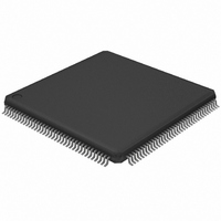
LPC2388FBD144,551 NXP Semiconductors, LPC2388FBD144,551 Datasheet - Page 32

LPC2388FBD144,551
Manufacturer Part Number
LPC2388FBD144,551
Description
IC ARM7 MCU FLASH 512K 144LQFP
Manufacturer
NXP Semiconductors
Series
LPC2300r
Specifications of LPC2388FBD144,551
Program Memory Type
FLASH
Program Memory Size
512KB (512K x 8)
Package / Case
144-LQFP
Core Processor
ARM7
Core Size
16/32-Bit
Speed
72MHz
Connectivity
CAN, EBI/EMI, Ethernet, I²C, Microwire, MMC, SPI, SSI, SSP, UART/USART, USB OTG
Peripherals
Brown-out Detect/Reset, DMA, I²S, POR, PWM, WDT
Number Of I /o
104
Ram Size
98K x 8
Voltage - Supply (vcc/vdd)
3 V ~ 3.6 V
Data Converters
A/D 8x10b; D/A 1x10b
Oscillator Type
Internal
Operating Temperature
-40°C ~ 85°C
Processor Series
LPC23
Core
ARM7TDMI-S
Data Bus Width
16 bit, 32 bit
Data Ram Size
98 KB
Interface Type
CAN/I2C/I2S/SPI/SSP/UART/USB
Maximum Clock Frequency
72 MHz
Number Of Programmable I/os
104
Number Of Timers
4
Operating Supply Voltage
3.3 V
Maximum Operating Temperature
+ 85 C
Mounting Style
SMD/SMT
3rd Party Development Tools
MDK-ARM, RL-ARM, ULINK2, MCB2388, MCB2388U, MCB2388UME
Development Tools By Supplier
OM11012
Minimum Operating Temperature
- 40 C
On-chip Adc
8-ch x 10-bit
On-chip Dac
1-ch x 10-bit
Lead Free Status / RoHS Status
Lead free / RoHS Compliant
For Use With
OM11012 - BOARD EVAL FOR LPC2388568-3999 - BOARD EVAL FOR LPC23 ARM MCU622-1005 - USB IN-CIRCUIT PROG ARM7 LPC2K
Eeprom Size
-
Lead Free Status / Rohs Status
Lead free / RoHS Compliant
Other names
568-4323
935285417551
LPC2388FBD144-S
935285417551
LPC2388FBD144-S
Available stocks
Company
Part Number
Manufacturer
Quantity
Price
Company:
Part Number:
LPC2388FBD144,551
Manufacturer:
NXP Semiconductors
Quantity:
10 000
NXP Semiconductors
LPC2388_0
Preliminary data sheet
7.25.3 Wake-up timer
7.25.4 Power control
Following the PLL input divider is the PLL multiplier. This can multiply the input divider
output through the use of a Current Controlled Oscillator (CCO) by a value ‘M’, in the
range of 1 through 32768. The resulting frequency must be in the range of 275 MHz to
550 MHz. The multiplier works by dividing the CCO output by the value of M, then using a
phase-frequency detector to compare the divided CCO output to the multiplier input. The
error value is used to adjust the CCO frequency.
The PLL is turned off and bypassed following a chip Reset and by entering Power-down
mode. PLL is enabled by software only. The program must configure and activate the PLL,
wait for the PLL to lock, then connect to the PLL as a clock source.
The LPC2388 begins operation at power-up and when awakened from Power-down mode
by using the 4 MHz IRC oscillator as the clock source. This allows chip operation to
resume quickly. If the main oscillator or the PLL is needed by the application, software will
need to enable these features and wait for them to stabilize before they are used as a
clock source.
When the main oscillator is initially activated, the wake-up timer allows software to ensure
that the main oscillator is fully functional before the processor uses it as a clock source
and starts to execute instructions. This is important at power on, all types of Reset, and
whenever any of the aforementioned functions are turned off for any reason. Since the
oscillator and other functions are turned off during Power-down mode, any wake-up of the
processor from Power-down mode makes use of the wake-up Timer.
The Wake-up Timer monitors the crystal oscillator to check whether it is safe to begin
code execution. When power is applied to the chip, or when some event caused the chip
to exit Power-down mode, some time is required for the oscillator to produce a signal of
sufficient amplitude to drive the clock logic. The amount of time depends on many factors,
including the rate of V
electrical characteristics (if a quartz crystal is used), as well as any other external circuitry
(e.g., capacitors), and the characteristics of the oscillator itself under the existing ambient
conditions.
The LPC2388 supports a variety of power control features. There are three special modes
of processor power reduction: Idle mode, Sleep mode, and Power-down mode. The CPU
clock rate may also be controlled as needed by changing clock sources, reconfiguring
PLL values, and/or altering the CPU clock divider value. This allows a trade-off of power
versus processing speed based on application requirements. In addition, Peripheral
Power Control allows shutting down the clocks to individual on-chip peripherals, allowing
fine tuning of power consumption by eliminating all dynamic power use in any peripherals
that are not required for the application. Each of the peripherals has its own clock divider
which provides even better power control.
The LPC2388 also implements a separate power domain in order to allow turning off
power to the bulk of the device while maintaining operation of the RTC and a small SRAM,
referred to as the Battery RAM.
Rev. 00.01 — 23 October 2007
DD(3V3)
ramp (in the case of power on), the type of crystal and its
Fast communication chip
LPC2388
© NXP B.V. 2007. All rights reserved.
32 of 57


