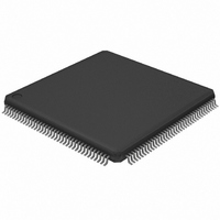
LPC2388FBD144,551 NXP Semiconductors, LPC2388FBD144,551 Datasheet - Page 7

LPC2388FBD144,551
Manufacturer Part Number
LPC2388FBD144,551
Description
IC ARM7 MCU FLASH 512K 144LQFP
Manufacturer
NXP Semiconductors
Series
LPC2300r
Specifications of LPC2388FBD144,551
Program Memory Type
FLASH
Program Memory Size
512KB (512K x 8)
Package / Case
144-LQFP
Core Processor
ARM7
Core Size
16/32-Bit
Speed
72MHz
Connectivity
CAN, EBI/EMI, Ethernet, I²C, Microwire, MMC, SPI, SSI, SSP, UART/USART, USB OTG
Peripherals
Brown-out Detect/Reset, DMA, I²S, POR, PWM, WDT
Number Of I /o
104
Ram Size
98K x 8
Voltage - Supply (vcc/vdd)
3 V ~ 3.6 V
Data Converters
A/D 8x10b; D/A 1x10b
Oscillator Type
Internal
Operating Temperature
-40°C ~ 85°C
Processor Series
LPC23
Core
ARM7TDMI-S
Data Bus Width
16 bit, 32 bit
Data Ram Size
98 KB
Interface Type
CAN/I2C/I2S/SPI/SSP/UART/USB
Maximum Clock Frequency
72 MHz
Number Of Programmable I/os
104
Number Of Timers
4
Operating Supply Voltage
3.3 V
Maximum Operating Temperature
+ 85 C
Mounting Style
SMD/SMT
3rd Party Development Tools
MDK-ARM, RL-ARM, ULINK2, MCB2388, MCB2388U, MCB2388UME
Development Tools By Supplier
OM11012
Minimum Operating Temperature
- 40 C
On-chip Adc
8-ch x 10-bit
On-chip Dac
1-ch x 10-bit
Lead Free Status / RoHS Status
Lead free / RoHS Compliant
For Use With
OM11012 - BOARD EVAL FOR LPC2388568-3999 - BOARD EVAL FOR LPC23 ARM MCU622-1005 - USB IN-CIRCUIT PROG ARM7 LPC2K
Eeprom Size
-
Lead Free Status / Rohs Status
Lead free / RoHS Compliant
Other names
568-4323
935285417551
LPC2388FBD144-S
935285417551
LPC2388FBD144-S
Available stocks
Company
Part Number
Manufacturer
Quantity
Price
Company:
Part Number:
LPC2388FBD144,551
Manufacturer:
NXP Semiconductors
Quantity:
10 000
NXP Semiconductors
Table 3.
LPC2388_0
Preliminary data sheet
Symbol
P0[14]/
USB_HSTEN2/
USB_CONNECT2/
SSEL1
P0[15]/TXD1/
SCK0/SCK
P0[16]/RXD1/
SSEL0/SSEL
P0[17]/CTS1/
MISO0/MISO
P0[18]/DCD1/
MOSI0/MOSI
P0[19]/DSR1/
MCICLK/SDA1
P0[20]/DTR1/
MCICMD/SCL1
P0[21]/RI1/
MCIPWR/RD1
P0[22]/RTS1/
MCIDAT0/TD1
Pin description
Pin
48
89
90
87
86
85
83
82
80
[1]
[1]
[1]
[1]
[1]
[1]
[1]
[1]
[1]
…continued
Type
I/O
O
O
I/O
I/O
O
I/O
I/O
I/O
I
I/O
I/O
I/O
I
I/O
I/O
I/O
I
I/O
I/O
I/O
I
O
I/O
I/O
O
I
I/O
I/O
I
O
I
I/O
O
O
O
Description
P0[14] — General purpose digital input/output pin.
USB_HSTEN2 — Host Enabled status for USB port 2.
USB_CONNECT2 — SoftConnect control for USB port 2. Signal used to switch an
external 1.5 kΩ resistor under software control. Used with the SoftConnect USB
feature.
SSEL1 — Slave Select for SSP1.
P0[15] — General purpose digital input/output pin.
TXD1 — Transmitter output for UART1.
SCK0 — Serial clock for SSP0.
SCK — Serial clock for SPI.
P0 [16] — General purpose digital input/output pin.
RXD1 — Receiver input for UART1.
SSEL0 — Slave Select for SSP0.
SSEL — Slave Select for SPI.
P0[17] — General purpose digital input/output pin.
CTS1 — Clear to Send input for UART1.
MISO0 — Master In Slave Out for SSP0.
MISO — Master In Slave Out for SPI.
P0[18] — General purpose digital input/output pin.
DCD1 — Data Carrier Detect input for UART1.
MOSI0 — Master Out Slave In for SSP0.
MOSI — Master Out Slave In for SPI.
P0[19] — General purpose digital input/output pin.
DSR1 — Data Set Ready input for UART1.
MCICLK — Clock output line for SD/MMC interface.
SDA1 — I
P0[20] — General purpose digital input/output pin.
DTR1 — Data Terminal Ready output for UART1.
MCICMD — Command line for SD/MMC interface.
SCL1 — I
P0[21] — General purpose digital input/output pin.
RI1 — Ring Indicator input for UART1.
MCIPWR — Power Supply Enable for external SD/MMC power supply.
RD1 — CAN1 receiver input.
P0[22] — General purpose digital input/output pin.
RTS1 — Request to Send output for UART1.
MCIDAT0 — Data line for SD/MMC interface.
TD1 — CAN1 transmitter output.
Rev. 00.01 — 23 October 2007
2
2
C1 clock input/output (this is not an open-drain pin).
C1 data input/output (this is not an open-drain pin).
Fast communication chip
LPC2388
© NXP B.V. 2007. All rights reserved.
7 of 57


