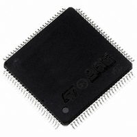
ST92F150CV1TB STMicroelectronics, ST92F150CV1TB Datasheet - Page 123

ST92F150CV1TB
Manufacturer Part Number
ST92F150CV1TB
Description
MCU 8BIT 128K FLASH 100TQFP
Manufacturer
STMicroelectronics
Series
ST9r
Datasheet
1.ST92F150CV1TB.pdf
(429 pages)
Specifications of ST92F150CV1TB
Core Processor
ST9
Core Size
8/16-Bit
Speed
24MHz
Connectivity
CAN, EBI/EMI, I²C, LIN, SCI, SPI
Peripherals
DMA, LVD, POR, PWM, WDT
Number Of I /o
77
Program Memory Size
128KB (128K x 8)
Program Memory Type
FLASH
Eeprom Size
1K x 8
Ram Size
4K x 8
Voltage - Supply (vcc/vdd)
4.5 V ~ 5.5 V
Data Converters
A/D 16x10b
Oscillator Type
Internal
Operating Temperature
-40°C ~ 105°C
Package / Case
100-TQFP, 100-VQFP
Processor Series
ST92F15x
Core
ST9
Data Bus Width
8 bit, 16 bit
Data Ram Size
6 KB
Interface Type
CAN, I2C, SCI, SPI
Maximum Clock Frequency
24 MHz
Number Of Programmable I/os
80
Number Of Timers
5 x 16 bit
Operating Supply Voltage
4.5 V to 5.5 V
Maximum Operating Temperature
+ 105 C
Mounting Style
SMD/SMT
Development Tools By Supplier
ST92F150-EPB
Minimum Operating Temperature
- 40 C
On-chip Adc
16 bit x 10 bit
Lead Free Status / RoHS Status
Lead free / RoHS Compliant
Other names
497-4883
Available stocks
Company
Part Number
Manufacturer
Quantity
Price
Company:
Part Number:
ST92F150CV1TB
Manufacturer:
STMicroelectronics
Quantity:
10 000
- Current page: 123 of 429
- Download datasheet (8Mb)
DMA TRANSACTIONS (Cont’d)
When selecting the DMA transaction with memory,
bit DCPR.RM (bit 0 of DCPR) must be cleared.
To select between using the ISR or the DMASR reg-
ister to extend the address, (see Memory Manage-
ment Unit chapter), the control bit DAPR.PS (bit 0
of DAPR) must be cleared or set respectively.
The DMA transaction Counter must be initialized
with the number of transactions to perform and will
be decremented after each transaction. The DMA
Address must be initialized with the starting ad-
dress of the DMA table and is increased after each
transaction. These two registers must be located
between addresses 00h and DFh of the Register
File.
Once a DMA channel is initialized, a transfer can
start. The direction of the transfer is automatically
defined by the type of peripheral and programming
mode.
Once the DMA table is completed (the transaction
counter reaches 0 value), an Interrupt request to
the CPU is generated.
Figure 58. DMA Between Memory and Peripheral
n
PAGED REGISTERS
PERIPHERAL
DCPR
DAPR
DATA
IDCR
IVR
ST92F124/F150/F250 - ON-CHIP DIRECT MEMORY ACCESS (DMA)
FFh
F0h
EFh
E0h
DFh
REGISTER FILE
TRANSACTION
REGISTERS
REGISTERS
COUNTER
ADDRESS
SYSTEM
PAGED
DMA TRANSACTION
DMA
DMA
When the Interrupt Pending (IDCR.IP) bit is set by
a hardware event (or by software), and the DMA
Mask bit (IDCR.DM) is set, a DMA request is gen-
erated. If the Priority Level of the DMA source is
higher than, or equal to, the Current Priority Level
(CPL), the DMA transfer is executed at the end of
the current instruction. DMA transfers read/write
data from/to the location pointed to by the DMA
Address Register, the DMA Address register is in-
cremented and the Transaction Counter Register
is decremented. When the contents of the Trans-
action Counter are decremented to zero, the DMA
Mask bit (DM) is cleared and an interrupt request
is generated, according to the Interrupt Mask bit
(End of Block interrupt). This End-of-Block inter-
rupt request is taken into account, depending on
the PRL value.
WARNING. DMA requests are not acknowledged
if the top level interrupt service is in progress.
000000h
000100h
SERVICE ROUTINE
TRANSFERRED
END OF BLOCK
ISR ADDRESS
INTERRUPT
ALREADY
MEMORY
DATA
VECTOR
TABLE
TABLE
DMA
123/429
9
Related parts for ST92F150CV1TB
Image
Part Number
Description
Manufacturer
Datasheet
Request
R

Part Number:
Description:
BOARD PROGRAM FOR ST92F150 MCU
Manufacturer:
STMicroelectronics
Datasheet:

Part Number:
Description:
BOARD EVALUATION FOR ST9 SERIES
Manufacturer:
STMicroelectronics
Datasheet:

Part Number:
Description:
BOARD EMULATOR FOR ST9 SERIES
Manufacturer:
STMicroelectronics
Datasheet:

Part Number:
Description:
MCU, MPU & DSP Development Tools ST9 Dedication Board
Manufacturer:
STMicroelectronics
Datasheet:

Part Number:
Description:
STMicroelectronics [RIPPLE-CARRY BINARY COUNTER/DIVIDERS]
Manufacturer:
STMicroelectronics
Datasheet:

Part Number:
Description:
STMicroelectronics [LIQUID-CRYSTAL DISPLAY DRIVERS]
Manufacturer:
STMicroelectronics
Datasheet:

Part Number:
Description:
BOARD EVAL FOR MEMS SENSORS
Manufacturer:
STMicroelectronics
Datasheet:

Part Number:
Description:
NPN TRANSISTOR POWER MODULE
Manufacturer:
STMicroelectronics
Datasheet:

Part Number:
Description:
TURBOSWITCH ULTRA-FAST HIGH VOLTAGE DIODE
Manufacturer:
STMicroelectronics
Datasheet:

Part Number:
Description:
Manufacturer:
STMicroelectronics
Datasheet:

Part Number:
Description:
DIODE / SCR MODULE
Manufacturer:
STMicroelectronics
Datasheet:

Part Number:
Description:
DIODE / SCR MODULE
Manufacturer:
STMicroelectronics
Datasheet:


