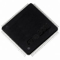
ST92F150CV1TB STMicroelectronics, ST92F150CV1TB Datasheet - Page 373

ST92F150CV1TB
Manufacturer Part Number
ST92F150CV1TB
Description
MCU 8BIT 128K FLASH 100TQFP
Manufacturer
STMicroelectronics
Series
ST9r
Datasheet
1.ST92F150CV1TB.pdf
(429 pages)
Specifications of ST92F150CV1TB
Core Processor
ST9
Core Size
8/16-Bit
Speed
24MHz
Connectivity
CAN, EBI/EMI, I²C, LIN, SCI, SPI
Peripherals
DMA, LVD, POR, PWM, WDT
Number Of I /o
77
Program Memory Size
128KB (128K x 8)
Program Memory Type
FLASH
Eeprom Size
1K x 8
Ram Size
4K x 8
Voltage - Supply (vcc/vdd)
4.5 V ~ 5.5 V
Data Converters
A/D 16x10b
Oscillator Type
Internal
Operating Temperature
-40°C ~ 105°C
Package / Case
100-TQFP, 100-VQFP
Processor Series
ST92F15x
Core
ST9
Data Bus Width
8 bit, 16 bit
Data Ram Size
6 KB
Interface Type
CAN, I2C, SCI, SPI
Maximum Clock Frequency
24 MHz
Number Of Programmable I/os
80
Number Of Timers
5 x 16 bit
Operating Supply Voltage
4.5 V to 5.5 V
Maximum Operating Temperature
+ 105 C
Mounting Style
SMD/SMT
Development Tools By Supplier
ST92F150-EPB
Minimum Operating Temperature
- 40 C
On-chip Adc
16 bit x 10 bit
Lead Free Status / RoHS Status
Lead free / RoHS Compliant
Other names
497-4883
Available stocks
Company
Part Number
Manufacturer
Quantity
Price
Company:
Part Number:
ST92F150CV1TB
Manufacturer:
STMicroelectronics
Quantity:
10 000
- Current page: 373 of 429
- Download datasheet (8Mb)
REGISTER DESCRIPTION (Cont’d)
Bit 4 = EXTG: External Trigger Enable.
This bit is set and cleared by software.
0: External trigger disabled.
1: External trigger enabled. Allows a conversion
Bit 3 = INTG: Internal Trigger Enable.
This bit is set and cleared by software.
0: Internal trigger disabled.
1: Internal trigger enabled. Allows a conversion se-
Both External and Internal Trigger inputs are inter-
nally ORed, thus avoiding Hardware conflicts;
however, the correct procedure is to enable only
one alternate synchronization input at a time.
Note: The effect of either synchronization mode is
to set the START/STOP bit, which is reset by hard-
ware when in SINGLE mode, at the end of each
sequence of conversions.
Requirements: The External Synchronisation In-
put must receive a low level pulse wider than an
INTCLK period and, for both External and On-Chip
Event synchronisation, the repetition period must
be greater than the time required for the selected
sequence of conversions.
Bit 2 = POW: Power Up/Power Down.
This bit is set and cleared by software.
0: Power down mode: all power-consuming logic is
1: Power up mode: the ADC converter logic and
Bit 1 = CONT: Continuous/Single.
0: Single Mode: a single sequence of conversions
1: Continuous Mode: the first sequence of conver-
sequence to be started on the subsequent edge
of the external signal applied to the EXTRG pin
(when enabled as an Alternate Function).
quence to be started, synchronized by an inter-
nal signal (On-chip Event signal) from a Multi-
function Timer peripheral.
disabled, thus selecting a low power idle mode.
analog circuitry is enabled.
is initiated whenever an external (or internal)
trigger occurs, or when the ST bit is set by soft-
ware.
sions is started, either by software (by setting
the ST bit), or by hardware (on an internal or ex-
ternal trigger, depending on the setting of the
INTG and EXTG bits); a continuous conversion
sequence is then initiated.
10-BIT ANALOG TO DIGITAL CONVERTER (ADC)
Bit 0 = ST: Start/Stop.
0: Stop conversion. When the ADC converter is
1: Start a sequence of conversions.
Note: If a write access to this register occurs, the
conversion is re-started from the SC[3:0] channel.
INTERRUPT CONTROL REGISTER (AD_ICR)
The Interrupt Control Register contains the three
priority level bits, the two source flags, and their bit
mask:
INTERRUPT CONTROL REGISTER (AD_ICR)
R254 - Read/Write
Register Page: 63
Reset Value: 0000 0111 (07h)
Bit 7 = ECV: End of Conversion.
This bit is automatically set by hardware after a
group of conversions is completed. It must be re-
set by the user, before returning from the Interrupt
Service Routine. Setting this bit by software will
cause a software interrupt request to be generat-
ed.
0: No End of Conversion event occurred
1: An End of Conversion event occurred
Bit 6 = AWD: Analog Watchdog.
This is automatically set by hardware whenever ei-
ther of the two monitored analog inputs exceeds a
threshold. The threshold values are stored in reg-
isters R244/R245 and R248/R249 for channel A,
and in registers R246/R247 and R250/R251 for
channel B respectively. The Compare Result Reg-
ister (CRR) keeps track of the analog inputs ex-
ceeding the thresholds.
The AWD bit must be reset by the user, before re-
turning from the Interrupt Service Routine. Setting
this bit by software will cause a software interrupt
request to be generated.
0: No Analog Watchdog event occurred
1: An Analog Watchdog event occurred
ECV AWD
running in Single Mode, this bit is hardware re-
set at the end of a sequence of conversions.
7
ECI AWDI
X
PL2
PL1
373/429
PL0
0
9
Related parts for ST92F150CV1TB
Image
Part Number
Description
Manufacturer
Datasheet
Request
R

Part Number:
Description:
BOARD PROGRAM FOR ST92F150 MCU
Manufacturer:
STMicroelectronics
Datasheet:

Part Number:
Description:
BOARD EVALUATION FOR ST9 SERIES
Manufacturer:
STMicroelectronics
Datasheet:

Part Number:
Description:
BOARD EMULATOR FOR ST9 SERIES
Manufacturer:
STMicroelectronics
Datasheet:

Part Number:
Description:
MCU, MPU & DSP Development Tools ST9 Dedication Board
Manufacturer:
STMicroelectronics
Datasheet:

Part Number:
Description:
STMicroelectronics [RIPPLE-CARRY BINARY COUNTER/DIVIDERS]
Manufacturer:
STMicroelectronics
Datasheet:

Part Number:
Description:
STMicroelectronics [LIQUID-CRYSTAL DISPLAY DRIVERS]
Manufacturer:
STMicroelectronics
Datasheet:

Part Number:
Description:
BOARD EVAL FOR MEMS SENSORS
Manufacturer:
STMicroelectronics
Datasheet:

Part Number:
Description:
NPN TRANSISTOR POWER MODULE
Manufacturer:
STMicroelectronics
Datasheet:

Part Number:
Description:
TURBOSWITCH ULTRA-FAST HIGH VOLTAGE DIODE
Manufacturer:
STMicroelectronics
Datasheet:

Part Number:
Description:
Manufacturer:
STMicroelectronics
Datasheet:

Part Number:
Description:
DIODE / SCR MODULE
Manufacturer:
STMicroelectronics
Datasheet:

Part Number:
Description:
DIODE / SCR MODULE
Manufacturer:
STMicroelectronics
Datasheet:


