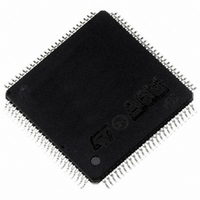
ST92F150CV1TB STMicroelectronics, ST92F150CV1TB Datasheet - Page 59

ST92F150CV1TB
Manufacturer Part Number
ST92F150CV1TB
Description
MCU 8BIT 128K FLASH 100TQFP
Manufacturer
STMicroelectronics
Series
ST9r
Datasheet
1.ST92F150CV1TB.pdf
(429 pages)
Specifications of ST92F150CV1TB
Core Processor
ST9
Core Size
8/16-Bit
Speed
24MHz
Connectivity
CAN, EBI/EMI, I²C, LIN, SCI, SPI
Peripherals
DMA, LVD, POR, PWM, WDT
Number Of I /o
77
Program Memory Size
128KB (128K x 8)
Program Memory Type
FLASH
Eeprom Size
1K x 8
Ram Size
4K x 8
Voltage - Supply (vcc/vdd)
4.5 V ~ 5.5 V
Data Converters
A/D 16x10b
Oscillator Type
Internal
Operating Temperature
-40°C ~ 105°C
Package / Case
100-TQFP, 100-VQFP
Processor Series
ST92F15x
Core
ST9
Data Bus Width
8 bit, 16 bit
Data Ram Size
6 KB
Interface Type
CAN, I2C, SCI, SPI
Maximum Clock Frequency
24 MHz
Number Of Programmable I/os
80
Number Of Timers
5 x 16 bit
Operating Supply Voltage
4.5 V to 5.5 V
Maximum Operating Temperature
+ 105 C
Mounting Style
SMD/SMT
Development Tools By Supplier
ST92F150-EPB
Minimum Operating Temperature
- 40 C
On-chip Adc
16 bit x 10 bit
Lead Free Status / RoHS Status
Lead free / RoHS Compliant
Other names
497-4883
Available stocks
Company
Part Number
Manufacturer
Quantity
Price
Company:
Part Number:
ST92F150CV1TB
Manufacturer:
STMicroelectronics
Quantity:
10 000
- Current page: 59 of 429
- Download datasheet (8Mb)
REGISTER DESCRIPTION (Cont’d)
The meaning of the FESSx bit for sector x is given
in
Table 10. Sector Status Bits
FLASH &
Address: 224003h /221003h-Read Only
Reset value: 0000 0000 (00h)
Bit 7 = ERER. Erase error (Read Only).
This bit is set by hardware when an Erase error oc-
curs during a Flash or an
This error is due to a real failure of a Flash cell,
that can no longer be erased. This kind of error is
fatal and the sector where it occurred must be dis-
carded. This bit is automatically cleared when bit
FEERR of the FESR0 register is cleared by soft-
ware.
0: Erase OK
1: Erase error
Bit 6 = PGER. Program error (Read Only).
This bit is automatically set when a Program error
occurs during a Flash or an
This error is due to a real failure of a Flash cell,
that can no longer be programmed. The byte
where this error occurred must be discarded (if it
was in the
grammed to FFh and then discarded, to avoid the
error occurring again when that byte is internally
moved). This bit is automatically cleared when bit
FEERR of the FESR0 register is cleared by soft-
ware.
0: Program OK
1: Flash or
ERER PGER SWER
FEERR
Table
7
1
0
0
0
ST92F124/F150/F250 - SINGLE VOLTAGE FLASH & E3 TM (EMULATED EEPROM)
10.
6
E
E
E
3 TM
FBUSY
EBUSY
3 TM
3 TM
1
0
0
-
5
STATUS REGISTER 1 (FESR1)
memory, the byte must be repro-
Programming error
4
FSUSP
1
0
-
-
3
E
E
3 TM
3 TM
on-going in sec-
Write operation
2
Suspended in
write operation.
Write Error in
write operation.
Sector Erase
Don’t care
FESSx=1
meaning
Sector x
sector x
tor x
1
0
Bit 5 = SWER. Swap or 1 over 0 Error (Read On-
ly).
This bit has two different meanings, depending on
whether the current write operation is to Flash or
E
In Flash memory this bit is automatically set when
trying to program at 1 bits previously set at 0 (this
does not happen when programming the Protec-
tion bits). This error is not due to a failure of the
Flash cell, but only flags that the desired data has
not been written.
In the
when a Program error occurs during the swapping
of the unselected pages to the new sector when
the old sector is full (see AN1152 for more details).
This error is due to a real failure of a Flash cell,
that can no longer be programmed. When this er-
ror is detected, the embedded algorithm automati-
cally exits the Page Update operation at the end of
the Swap phase, without performing the Erase
Phase 0 on the full sector. In this way the old data
are kept, and through predefined routines in Test-
Flash (Find Wrong Pages = 230029h and Find
Wrong Bytes = 23002Ch), the user can compare
the old and the new data to find where the error oc-
curred.
Once the error has been discovered the user must
take to end the stopped Erase Phase 0 on the old
sector (through another predefined routine in Test-
Flash:
where the error occurred must be reprogrammed
to FFh and then discarded, to avoid the error oc-
curring again when that byte is internally moved.
This bit is automatically cleared when bit FEERR
of the FESR0 register is cleared by software.
Bit 4:0 = Reserved.
3 TM
memory.
E
Complete Swap = 23002Fh). The byte
3 TM
memory this bit is automatically set
59/429
9
Related parts for ST92F150CV1TB
Image
Part Number
Description
Manufacturer
Datasheet
Request
R

Part Number:
Description:
BOARD PROGRAM FOR ST92F150 MCU
Manufacturer:
STMicroelectronics
Datasheet:

Part Number:
Description:
BOARD EVALUATION FOR ST9 SERIES
Manufacturer:
STMicroelectronics
Datasheet:

Part Number:
Description:
BOARD EMULATOR FOR ST9 SERIES
Manufacturer:
STMicroelectronics
Datasheet:

Part Number:
Description:
MCU, MPU & DSP Development Tools ST9 Dedication Board
Manufacturer:
STMicroelectronics
Datasheet:

Part Number:
Description:
STMicroelectronics [RIPPLE-CARRY BINARY COUNTER/DIVIDERS]
Manufacturer:
STMicroelectronics
Datasheet:

Part Number:
Description:
STMicroelectronics [LIQUID-CRYSTAL DISPLAY DRIVERS]
Manufacturer:
STMicroelectronics
Datasheet:

Part Number:
Description:
BOARD EVAL FOR MEMS SENSORS
Manufacturer:
STMicroelectronics
Datasheet:

Part Number:
Description:
NPN TRANSISTOR POWER MODULE
Manufacturer:
STMicroelectronics
Datasheet:

Part Number:
Description:
TURBOSWITCH ULTRA-FAST HIGH VOLTAGE DIODE
Manufacturer:
STMicroelectronics
Datasheet:

Part Number:
Description:
Manufacturer:
STMicroelectronics
Datasheet:

Part Number:
Description:
DIODE / SCR MODULE
Manufacturer:
STMicroelectronics
Datasheet:

Part Number:
Description:
DIODE / SCR MODULE
Manufacturer:
STMicroelectronics
Datasheet:


