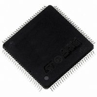
ST92F150CV1TB STMicroelectronics, ST92F150CV1TB Datasheet - Page 204

ST92F150CV1TB
Manufacturer Part Number
ST92F150CV1TB
Description
MCU 8BIT 128K FLASH 100TQFP
Manufacturer
STMicroelectronics
Series
ST9r
Datasheet
1.ST92F150CV1TB.pdf
(429 pages)
Specifications of ST92F150CV1TB
Core Processor
ST9
Core Size
8/16-Bit
Speed
24MHz
Connectivity
CAN, EBI/EMI, I²C, LIN, SCI, SPI
Peripherals
DMA, LVD, POR, PWM, WDT
Number Of I /o
77
Program Memory Size
128KB (128K x 8)
Program Memory Type
FLASH
Eeprom Size
1K x 8
Ram Size
4K x 8
Voltage - Supply (vcc/vdd)
4.5 V ~ 5.5 V
Data Converters
A/D 16x10b
Oscillator Type
Internal
Operating Temperature
-40°C ~ 105°C
Package / Case
100-TQFP, 100-VQFP
Processor Series
ST92F15x
Core
ST9
Data Bus Width
8 bit, 16 bit
Data Ram Size
6 KB
Interface Type
CAN, I2C, SCI, SPI
Maximum Clock Frequency
24 MHz
Number Of Programmable I/os
80
Number Of Timers
5 x 16 bit
Operating Supply Voltage
4.5 V to 5.5 V
Maximum Operating Temperature
+ 105 C
Mounting Style
SMD/SMT
Development Tools By Supplier
ST92F150-EPB
Minimum Operating Temperature
- 40 C
On-chip Adc
16 bit x 10 bit
Lead Free Status / RoHS Status
Lead free / RoHS Compliant
Other names
497-4883
Available stocks
Company
Part Number
Manufacturer
Quantity
Price
Company:
Part Number:
ST92F150CV1TB
Manufacturer:
STMicroelectronics
Quantity:
10 000
- Current page: 204 of 429
- Download datasheet (8Mb)
MULTIFUNCTION TIMER (MFT)
MULTIFUNCTION TIMER (Cont’d)
TIMER MODE REGISTER (TMR)
R249 - Read/Write
Register Page: 10
Reset value: 0000 0000 (00h)
Bit 7 = OE1: Output 1 enable.
0: Disable the Output 1 (TxOUTB pin) and force it
1: Enable the Output 1 (TxOUTB pin)
Bit 6 = OE0: Output 0 enable.
0: Disable the Output 0 (TxOUTA pin) and force it
1: Enable the Output 0 (TxOUTA pin).
Bit 5 = BM: Bivalue mode.
This bit works together with the RM1 and RM0 bits
to select the timer operating mode (see
0: Disable bivalue mode
1: Enable bivalue mode
Bit 4 = RM1: REG1R mode.
This bit works together with the BM and RM0 bits
to select the timer operating mode. Refer to
41.
Note: This bit has no effect when the Bivalue
Mode is enabled (BM=1).
204/429
9
OE1
high.
The relevant I/O bit must also be set to Alternate
Function
high
The relevant I/O bit must also be set to Alternate
Function
7
OE0
BM
RM1 RM0 ECK REN
Table
Table
C0
41).
0
Bit 3 = RM0: REG0R mode.
This bit works together with the BM and RM1 bits
to select the timer operating mode. Refer to
41.
Table 41. Timer Operating Modes
Bit 2 = ECK Timer clock control.
0: The prescaler clock source is selected depend-
1: Enter Parallel mode (for Timer 1 and Timer 3
Bit 1 = REN: Retrigger mode.
0: Enable retriggerable mode
1: Disable retriggerable mode
Bit 0 = CO: Continous/One shot mode.
0: Continuous mode (with autoreload on End of
1: One shot mode
BM RM1 RM0
1
1
0
0
0
0
ing on the IN0 - IN3 bits in the T_ICR register
only, no effect for Timer 0 and 2). See
10.4.2.12.
Count condition)
TMR Bits
x
x
0
1
0
1
0
1
0
0
1
1
Biload mode
Bicapture mode
Load from REG0R and Monitor on
REG1R
Load from REG0R and Capture on
REG1R
Capture on REG0R and Monitor on
REG1R
Capture on REG0R and REG1R
Timer Operating Modes
Section
Table
Related parts for ST92F150CV1TB
Image
Part Number
Description
Manufacturer
Datasheet
Request
R

Part Number:
Description:
BOARD PROGRAM FOR ST92F150 MCU
Manufacturer:
STMicroelectronics
Datasheet:

Part Number:
Description:
BOARD EVALUATION FOR ST9 SERIES
Manufacturer:
STMicroelectronics
Datasheet:

Part Number:
Description:
BOARD EMULATOR FOR ST9 SERIES
Manufacturer:
STMicroelectronics
Datasheet:

Part Number:
Description:
MCU, MPU & DSP Development Tools ST9 Dedication Board
Manufacturer:
STMicroelectronics
Datasheet:

Part Number:
Description:
STMicroelectronics [RIPPLE-CARRY BINARY COUNTER/DIVIDERS]
Manufacturer:
STMicroelectronics
Datasheet:

Part Number:
Description:
STMicroelectronics [LIQUID-CRYSTAL DISPLAY DRIVERS]
Manufacturer:
STMicroelectronics
Datasheet:

Part Number:
Description:
BOARD EVAL FOR MEMS SENSORS
Manufacturer:
STMicroelectronics
Datasheet:

Part Number:
Description:
NPN TRANSISTOR POWER MODULE
Manufacturer:
STMicroelectronics
Datasheet:

Part Number:
Description:
TURBOSWITCH ULTRA-FAST HIGH VOLTAGE DIODE
Manufacturer:
STMicroelectronics
Datasheet:

Part Number:
Description:
Manufacturer:
STMicroelectronics
Datasheet:

Part Number:
Description:
DIODE / SCR MODULE
Manufacturer:
STMicroelectronics
Datasheet:

Part Number:
Description:
DIODE / SCR MODULE
Manufacturer:
STMicroelectronics
Datasheet:


