MCHC912B32CFUE8 Freescale Semiconductor, MCHC912B32CFUE8 Datasheet - Page 282
MCHC912B32CFUE8
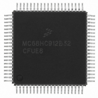
Manufacturer Part Number
MCHC912B32CFUE8
Description
IC MCU 32K FLASH 8MHZ 80-QFP
Manufacturer
Freescale Semiconductor
Series
HC12r
Datasheet
1.MCHC912B32CFUE8.pdf
(334 pages)
Specifications of MCHC912B32CFUE8
Core Processor
CPU12
Core Size
16-Bit
Speed
8MHz
Connectivity
SCI, SPI
Peripherals
POR, PWM, WDT
Number Of I /o
63
Program Memory Size
32KB (32K x 8)
Program Memory Type
FLASH
Eeprom Size
768 x 8
Ram Size
1K x 8
Voltage - Supply (vcc/vdd)
4.5 V ~ 5.5 V
Data Converters
A/D 8x10b
Oscillator Type
External
Operating Temperature
-40°C ~ 85°C
Package / Case
80-QFP
Cpu Family
HC12
Device Core Size
16b
Frequency (max)
8MHz
Interface Type
SCI/SPI
Total Internal Ram Size
1KB
# I/os (max)
63
Operating Supply Voltage (typ)
5V
Operating Supply Voltage (max)
5.5V
Operating Supply Voltage (min)
4.5V
On-chip Adc
8-chx10-bit
Instruction Set Architecture
CISC
Operating Temp Range
-40C to 85C
Operating Temperature Classification
Industrial
Mounting
Surface Mount
Pin Count
80
Package Type
PQFP
Package
80PQFP
Family Name
HC12
Maximum Speed
8 MHz
Operating Supply Voltage
5 V
Data Bus Width
16 Bit
Number Of Programmable I/os
63
Processor Series
HC912B
Core
HC12
Data Ram Size
1 KB
Maximum Clock Frequency
8 MHz
Maximum Operating Temperature
+ 85 C
Mounting Style
SMD/SMT
3rd Party Development Tools
EWHCS12
Development Tools By Supplier
M68EVB912B32E
Minimum Operating Temperature
- 40 C
Lead Free Status / RoHS Status
Lead free / RoHS Compliant
Available stocks
Company
Part Number
Manufacturer
Quantity
Price
Company:

Part Number:
MCHC912B32CFUE8
Manufacturer:
Freescale Semiconductor
Quantity:
10 000


Analog-to-Digital Converter (ATD)
17.3.6 ATD Control Register 5
Read: Anytime
Write: Anytime
The ATD control register 5 is used to select the conversion modes, the conversion channel(s), and initiate
conversions.
A write to ATDCTL5 initiates a new conversion sequence. If a conversion sequence is in progress when
a write occurs, that sequence is aborted and the SCF and CCF bits are reset.
S8CM — Select 8 Channel Mode Bit
282
Clearing these bits causes the prescale value to default to 1 which results in a divide-by-two prescale
factor. This signal is then fed into the divide-by-two logic. The reset state divides the P clock by a total
of four and is appropriate for nominal operation at a bus rate of between 2 MHz and 8 MHz.
shows the divide-by operation and the appropriate range of system clock frequencies.
0 = Conversion sequence consists of four conversions.
1 = Conversion sequence consists of eight conversions.
Reset:
Address: $0065
Read:
Write:
1. Maximum conversion frequency is 2 MHz. Maximum P clock divisor value becomes
2. Minimum conversion frequency is 500 kHz. Minimum P clock divisor value becomes
Prescale Value
maximum conversion rate that can be used on this ATD module.
minimum conversion rate that this ATD can perform.
00000
00001
00010
00011
00100
00101
00110
00111
01xxx
1xxxx
Bit 7
0
Figure 17-7. ATD Control Register 5 (ATDCTL5)
= Unimplemented
S8CM
Table 17-3. Clock Prescaler Values
6
0
M68HC12B Family Data Sheet, Rev. 9.1
Total Divisor
SCAN
10
12
14
16
2
4
6
8
5
0
MULT
4
0
Max P Clock
Do not use
4 MHz
8 MHz
8 MHz
8 MHz
8 MHz
8 MHz
8 MHz
8 MHz
CD
3
0
(1)
CC
2
0
Min P Clock
1 MHz
2 MHz
3 MHz
4 MHz
5 MHz
6 MHz
7 MHz
8 MHz
CB
1
0
Freescale Semiconductor
(2)
Bit 0
CA
0
Table 17-3
Related parts for MCHC912B32CFUE8
Image
Part Number
Description
Manufacturer
Datasheet
Request
R

Part Number:
Description:
Manufacturer:
Freescale Semiconductor, Inc
Datasheet:
Part Number:
Description:
Manufacturer:
Freescale Semiconductor, Inc
Datasheet:
Part Number:
Description:
Manufacturer:
Freescale Semiconductor, Inc
Datasheet:
Part Number:
Description:
Manufacturer:
Freescale Semiconductor, Inc
Datasheet:
Part Number:
Description:
Manufacturer:
Freescale Semiconductor, Inc
Datasheet:
Part Number:
Description:
Manufacturer:
Freescale Semiconductor, Inc
Datasheet:
Part Number:
Description:
Manufacturer:
Freescale Semiconductor, Inc
Datasheet:
Part Number:
Description:
Manufacturer:
Freescale Semiconductor, Inc
Datasheet:
Part Number:
Description:
Manufacturer:
Freescale Semiconductor, Inc
Datasheet:
Part Number:
Description:
Manufacturer:
Freescale Semiconductor, Inc
Datasheet:
Part Number:
Description:
Manufacturer:
Freescale Semiconductor, Inc
Datasheet:
Part Number:
Description:
Manufacturer:
Freescale Semiconductor, Inc
Datasheet:
Part Number:
Description:
Manufacturer:
Freescale Semiconductor, Inc
Datasheet:
Part Number:
Description:
Manufacturer:
Freescale Semiconductor, Inc
Datasheet:
Part Number:
Description:
Manufacturer:
Freescale Semiconductor, Inc
Datasheet: