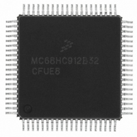
MCHC912B32CFUE8 Freescale Semiconductor, MCHC912B32CFUE8 Datasheet - Page 31

MCHC912B32CFUE8
Manufacturer Part Number
MCHC912B32CFUE8
Description
IC MCU 32K FLASH 8MHZ 80-QFP
Manufacturer
Freescale Semiconductor
Series
HC12r
Datasheet
1.MCHC912B32CFUE8.pdf
(334 pages)
Specifications of MCHC912B32CFUE8
Core Processor
CPU12
Core Size
16-Bit
Speed
8MHz
Connectivity
SCI, SPI
Peripherals
POR, PWM, WDT
Number Of I /o
63
Program Memory Size
32KB (32K x 8)
Program Memory Type
FLASH
Eeprom Size
768 x 8
Ram Size
1K x 8
Voltage - Supply (vcc/vdd)
4.5 V ~ 5.5 V
Data Converters
A/D 8x10b
Oscillator Type
External
Operating Temperature
-40°C ~ 85°C
Package / Case
80-QFP
Cpu Family
HC12
Device Core Size
16b
Frequency (max)
8MHz
Interface Type
SCI/SPI
Total Internal Ram Size
1KB
# I/os (max)
63
Operating Supply Voltage (typ)
5V
Operating Supply Voltage (max)
5.5V
Operating Supply Voltage (min)
4.5V
On-chip Adc
8-chx10-bit
Instruction Set Architecture
CISC
Operating Temp Range
-40C to 85C
Operating Temperature Classification
Industrial
Mounting
Surface Mount
Pin Count
80
Package Type
PQFP
Package
80PQFP
Family Name
HC12
Maximum Speed
8 MHz
Operating Supply Voltage
5 V
Data Bus Width
16 Bit
Number Of Programmable I/os
63
Processor Series
HC912B
Core
HC12
Data Ram Size
1 KB
Maximum Clock Frequency
8 MHz
Maximum Operating Temperature
+ 85 C
Mounting Style
SMD/SMT
3rd Party Development Tools
EWHCS12
Development Tools By Supplier
M68EVB912B32E
Minimum Operating Temperature
- 40 C
Lead Free Status / RoHS Status
Lead free / RoHS Compliant
Available stocks
Company
Part Number
Manufacturer
Quantity
Price
Company:
Part Number:
MCHC912B32CFUE8
Manufacturer:
Freescale Semiconductor
Quantity:
10 000
- Current page: 31 of 334
- Download datasheet (2Mb)
Freescale Semiconductor
1. The RxCAN and TxCAN designations are for the MC68HC(9)12BC32 only.
ADDR15–ADDR8
DLCRx/RxCAN
DLCTx/TxCAN
ADDR7–ADDR0
DATA15–DATA8
IPIPE1, IPIPE0
MODB, MODA
DATA7–DATA0
IOC7–IOC0
SDO/MOSI
PW3–PW0
AN7–AN0
SDI/MISO
RESET
LSTRB
TAGLO
EXTAL
CS/SS
BKGD
TAGHI
Name
ECLK
XIRQ
RxD0
XTAL
TxD0
DBE
SCK
R/W
IRQ
Pin
PAI
(1)
(1)
16–12, 9–7
Number
25–18
46–39
58–51
27, 28
27, 28
3–6
Pin
16
26
29
32
33
34
35
35
36
37
38
17
17
76
75
68
67
66
65
62
61
Table 1-3. Signal Description Summary
Pulse-width modulator channel outputs
External bus pins share function with general-purpose I/O ports A and B. In single-chip
modes, the pins can be used for I/O. In expanded modes, the pins are used for the
external buses.
Pins used for input capture and output compare in the timer and pulse accumulator
subsystem
Pulse accumulator input
Analog inputs for the analog-to-digital conversion module
Data bus control and, in expanded mode, enables the drive control of external buses
during external reads
State of mode select pins during reset determines the initial operating mode of the
MCU. After reset, MODB and MODA can be configured as instruction queue tracking
signals IPIPE1 and IPIPE0 or as general-purpose I/O pins.
E-clock is the output connection for the external bus clock. ECLK is used as a timing
reference and for address demultiplexing.
An active low bidirectional control signal, RESET acts as an input to initialize the MCU
to a known startup state and an output when COP or clock monitor causes a reset.
Crystal driver and external clock input pins. On reset all the device clocks are derived
from the EXTAL input frequency. XTAL is the crystal output.
Low byte strobe (0 = low byte valid), in all modes this pin can be used as I/O. The low
strobe function is the exclusive-NOR of A0 and the internal SZ8 signal. The SZ8
internal signal indicates the size 16/8 access.
Pin used in instruction tagging
Indicates direction of data on expansion bus; shares function with general-purpose I/O;
read/write in expanded modes
Maskable interrupt request input provides a means of applying asynchronous interrupt
requests to the MCU. Either falling edge-sensitive triggering or level-sensitive
triggering is program selectable (INTCR register).
Provides a means of requesting asynchronous non-maskable interrupt requests after
reset initialization
Single-wire background interface pin is dedicated to the background debug function.
During reset, this pin determines special or normal operating mode.
Pin used in instruction tagging
BDLC receive pin
BDLC transmit pin
Slave-select output for SPI master mode; input for slave mode or master mode
Serial clock for SPI system
Master out/slave in pin for serial peripheral interface
Master in/slave out pin for serial peripheral interface
SCI transmit pin
SCI receive pin
M68HC12B Family Data Sheet, Rev. 9.1
Description
Pinout and Signal Descriptions
31
Related parts for MCHC912B32CFUE8
Image
Part Number
Description
Manufacturer
Datasheet
Request
R
Part Number:
Description:
Manufacturer:
Freescale Semiconductor, Inc
Datasheet:
Part Number:
Description:
Manufacturer:
Freescale Semiconductor, Inc
Datasheet:
Part Number:
Description:
Manufacturer:
Freescale Semiconductor, Inc
Datasheet:
Part Number:
Description:
Manufacturer:
Freescale Semiconductor, Inc
Datasheet:
Part Number:
Description:
Manufacturer:
Freescale Semiconductor, Inc
Datasheet:
Part Number:
Description:
Manufacturer:
Freescale Semiconductor, Inc
Datasheet:
Part Number:
Description:
Manufacturer:
Freescale Semiconductor, Inc
Datasheet:
Part Number:
Description:
Manufacturer:
Freescale Semiconductor, Inc
Datasheet:
Part Number:
Description:
Manufacturer:
Freescale Semiconductor, Inc
Datasheet:
Part Number:
Description:
Manufacturer:
Freescale Semiconductor, Inc
Datasheet:
Part Number:
Description:
Manufacturer:
Freescale Semiconductor, Inc
Datasheet:
Part Number:
Description:
Manufacturer:
Freescale Semiconductor, Inc
Datasheet:
Part Number:
Description:
Manufacturer:
Freescale Semiconductor, Inc
Datasheet:
Part Number:
Description:
Manufacturer:
Freescale Semiconductor, Inc
Datasheet:
Part Number:
Description:
Manufacturer:
Freescale Semiconductor, Inc
Datasheet:


