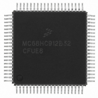
MCHC912B32CFUE8 Freescale Semiconductor, MCHC912B32CFUE8 Datasheet - Page 316

MCHC912B32CFUE8
Manufacturer Part Number
MCHC912B32CFUE8
Description
IC MCU 32K FLASH 8MHZ 80-QFP
Manufacturer
Freescale Semiconductor
Series
HC12r
Datasheet
1.MCHC912B32CFUE8.pdf
(334 pages)
Specifications of MCHC912B32CFUE8
Core Processor
CPU12
Core Size
16-Bit
Speed
8MHz
Connectivity
SCI, SPI
Peripherals
POR, PWM, WDT
Number Of I /o
63
Program Memory Size
32KB (32K x 8)
Program Memory Type
FLASH
Eeprom Size
768 x 8
Ram Size
1K x 8
Voltage - Supply (vcc/vdd)
4.5 V ~ 5.5 V
Data Converters
A/D 8x10b
Oscillator Type
External
Operating Temperature
-40°C ~ 85°C
Package / Case
80-QFP
Cpu Family
HC12
Device Core Size
16b
Frequency (max)
8MHz
Interface Type
SCI/SPI
Total Internal Ram Size
1KB
# I/os (max)
63
Operating Supply Voltage (typ)
5V
Operating Supply Voltage (max)
5.5V
Operating Supply Voltage (min)
4.5V
On-chip Adc
8-chx10-bit
Instruction Set Architecture
CISC
Operating Temp Range
-40C to 85C
Operating Temperature Classification
Industrial
Mounting
Surface Mount
Pin Count
80
Package Type
PQFP
Package
80PQFP
Family Name
HC12
Maximum Speed
8 MHz
Operating Supply Voltage
5 V
Data Bus Width
16 Bit
Number Of Programmable I/os
63
Processor Series
HC912B
Core
HC12
Data Ram Size
1 KB
Maximum Clock Frequency
8 MHz
Maximum Operating Temperature
+ 85 C
Mounting Style
SMD/SMT
3rd Party Development Tools
EWHCS12
Development Tools By Supplier
M68EVB912B32E
Minimum Operating Temperature
- 40 C
Lead Free Status / RoHS Status
Lead free / RoHS Compliant
Available stocks
Company
Part Number
Manufacturer
Quantity
Price
Company:
Part Number:
MCHC912B32CFUE8
Manufacturer:
Freescale Semiconductor
Quantity:
10 000
- Current page: 316 of 334
- Download datasheet (2Mb)
Electrical Specifications
19.12.2 Example V
Figure 19-2
voltage levels on the V
intended to do, and some design considerations when designing V
The general idea of this circuit implementation is to supply V
converter, like most, provides a shutdown feature which allows the converter’s output to be shut off. When
the SHDN pin on the converter is pulled high, as the 10-kΩ pullup resistor (R1) does, the output V
shorted to the V
the MCU to turn on the converter and supply the 12-volt programming voltage during the programming or
erasing cycle. Simple programming and erasing routines, such as those shown earlier in this application
note, will no longer suffice.
By implementing this solution, V
and fall together. Capacitors C5 and C6 are the normal decoupling capacitors on the V
C3 is used to reduce electromagnetic interference (EMI) in the circuit. If C3 is too large, V
allowed to fall with V
C4 is where the dc-dc converter stores charge to supply V
able to source approximately 30 mA of current for at least 20 µs (based on programming cycle
requirements) and 4 mA of current for at least 10 ms (based on erase cycle requirements).
A certain degree of experimentation might be required when selecting C4 and C3. When trying different
capacitor values, always monitor the effects on V
V
R1 must be no larger than 10 kΩ, to make certain that the SHDN pin on the dc-dc converter is never
allowed to fall below V
ensures this behavior, no matter what port pin is used on the microcontroller or what the internal structure
of that pin looks like. Without a strong enough pullup resistor on R1, the voltage on the SHDN pin might
drop during a reset event, causing the dc-dc converter to activate and begin driving the voltage on V
to begin to rise to 12 volts. This would result in data corruption in the FLASH.
316
FP
pin.
shows an example of a circuit which, if properly implemented, can maintain the appropriate
220 nF
220 nF
DD
supply. This requires that the programming and erasing routines assert a port pin on
DD
FP
DD
5
2
1
4
3
FP
, potentially causing data corruption in the FLASH array. (Refer to
V
C1+
C1 –
C2+
C2–
Protection Circuitry
unless the output pin of the microcontroller is driven low. The external pullup
pin. This section outlines the design for this circuit, what each component is
DD
ST662A
GND
7
FP
SHDN
V
OUT
is tied to V
M68HC12B Family Data Sheet, Rev. 9.1
Figure 19-2. V
6
8
C4
C3
10 µF
1–100 nF
DD
FP
on power-up and power-down, ensuring that they rise
FP
decay during power-down and current supplied to the
Supply Circuit
V
DD
R1 10 kΩ
Out
C5
FP
to the target device. The supply must be
V
FP
from a dc-dc converter. This dc-dc
10 µF
SHUTDOWN
FP
pin protection.
C6
100 nF
V
V
I/O
V
Freescale Semiconductor
DD
FP
SS
DD
FP
Figure
supply lines.
will not be
19-3.)
Out
Out
is
Related parts for MCHC912B32CFUE8
Image
Part Number
Description
Manufacturer
Datasheet
Request
R
Part Number:
Description:
Manufacturer:
Freescale Semiconductor, Inc
Datasheet:
Part Number:
Description:
Manufacturer:
Freescale Semiconductor, Inc
Datasheet:
Part Number:
Description:
Manufacturer:
Freescale Semiconductor, Inc
Datasheet:
Part Number:
Description:
Manufacturer:
Freescale Semiconductor, Inc
Datasheet:
Part Number:
Description:
Manufacturer:
Freescale Semiconductor, Inc
Datasheet:
Part Number:
Description:
Manufacturer:
Freescale Semiconductor, Inc
Datasheet:
Part Number:
Description:
Manufacturer:
Freescale Semiconductor, Inc
Datasheet:
Part Number:
Description:
Manufacturer:
Freescale Semiconductor, Inc
Datasheet:
Part Number:
Description:
Manufacturer:
Freescale Semiconductor, Inc
Datasheet:
Part Number:
Description:
Manufacturer:
Freescale Semiconductor, Inc
Datasheet:
Part Number:
Description:
Manufacturer:
Freescale Semiconductor, Inc
Datasheet:
Part Number:
Description:
Manufacturer:
Freescale Semiconductor, Inc
Datasheet:
Part Number:
Description:
Manufacturer:
Freescale Semiconductor, Inc
Datasheet:
Part Number:
Description:
Manufacturer:
Freescale Semiconductor, Inc
Datasheet:
Part Number:
Description:
Manufacturer:
Freescale Semiconductor, Inc
Datasheet:


