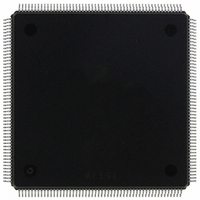
MCF5407AI220 Freescale Semiconductor, MCF5407AI220 Datasheet - Page 314

MCF5407AI220
Manufacturer Part Number
MCF5407AI220
Description
IC MPU 32B 220MHZ COLDF 208-FQFP
Manufacturer
Freescale Semiconductor
Series
MCF540xr
Specifications of MCF5407AI220
Core Processor
Coldfire V4
Core Size
32-Bit
Speed
220MHz
Connectivity
EBI/EMI, I²C, UART/USART
Peripherals
DMA, WDT
Number Of I /o
16
Program Memory Type
ROMless
Ram Size
4K x 8
Voltage - Supply (vcc/vdd)
1.65 V ~ 3.6 V
Oscillator Type
External
Operating Temperature
0°C ~ 70°C
Package / Case
208-FQFP
Maximum Clock Frequency
220 MHz
Operating Supply Voltage
1.8 V, 3.3 V
Maximum Operating Temperature
+ 105 C
Mounting Style
SMD/SMT
Minimum Operating Temperature
0 C
Program Memory Size
24KB
Cpu Speed
220MHz
Embedded Interface Type
I2C, UART
Digital Ic Case Style
FQFP
No. Of Pins
208
Supply Voltage Range
3.3V
Rohs Compliant
Yes
For Use With
M5407C3 - KIT EVAL FOR MCF5407 W/ETHERNET
Lead Free Status / RoHS Status
Lead free / RoHS Compliant
Eeprom Size
-
Program Memory Size
-
Data Converters
-
Lead Free Status / Rohs Status
Lead free / RoHS Compliant
Available stocks
Company
Part Number
Manufacturer
Quantity
Price
Company:
Part Number:
MCF5407AI220
Manufacturer:
freescaie
Quantity:
6
Company:
Part Number:
MCF5407AI220
Manufacturer:
Freescale Semiconductor
Quantity:
135
Company:
Part Number:
MCF5407AI220
Manufacturer:
FREESCALE
Quantity:
1 831
Company:
Part Number:
MCF5407AI220
Manufacturer:
Freescale Semiconductor
Quantity:
10 000
- Current page: 314 of 546
- Download datasheet (7Mb)
DMA Signal Description
12.1.1 DMA Module Features
The DMA controller module features are as follows:
12.2 DMA Signal Description
Table 12-1 briefly describes the DMA module signals that provide handshake control for
either a source or destination external device.
12-2
DREQ[1:0]/
PP[6:5]
TT[1:0]/
PP[1:0]
Signal
• Four fully independent, programmable DMA controller channels/bus modules
• Auto-alignment feature for source or destination accesses
• Dual- and single-address transfers
• Two external request pins (DREQ[1:0]) provided for channels 1 and 0
• Two external acknowledge pins (DACK[1:0]) provided for channels 1 and 0
• Channels 2 and 3 have request signals connected to the interrupt lines of UART0 and
• Channel arbitration on transfer boundaries
• Data transfers in 8-, 16-, 32-, or 128-bit blocks using a 16-byte buffer
• Continuous-mode and cycle-steal transfers
• Independent transfer widths for source and destination
• Independent source and destination address registers
• Data transfer can occur in as few as two clocks
UART1, programmable through the channel select field MODCTL[DSL]. See
Section 14.3.4, “Modem Control Register (MODCTL).”
I/O
O
I
External DMA request. DREQ[1:0] can serve as the DMA request inputs or as two parallel port
bits. They are programmable individually through the PAR. A peripheral device asserts these
inputs to request an operand transfer between it and memory.
DREQ signals are asserted to initiate DMA accesses in the respective channels. The system
should drive unused DREQ signals to logic high. Although each channel has an individual
DREQ signal, in the MCF5407 only channels 0 and 1 connect to external DREQ pins. DREQ2
and DREQ3 are programmable for use with UART0 and UART1 through MODCTL[DSL]. See
Section 14.3.4, “Modem Control Register (MODCTL).”
Transfer type. A DMA access is indicated by the transfer type pins, TT[1:0] = 01. The transfer
modifier, TM[2:0], and DMA acknowledgement, DACK[1:0], configurations shown below are
meaningful only if TT[1:0] = 01, indicating an external master or DMA access.
Table 12-1. DMA Signals
MCF5407 User’s Manual
Description
Related parts for MCF5407AI220
Image
Part Number
Description
Manufacturer
Datasheet
Request
R
Part Number:
Description:
Mcf5407 Coldfire Integrated Microprocessor User
Manufacturer:
Freescale Semiconductor, Inc
Datasheet:
Part Number:
Description:
Manufacturer:
Freescale Semiconductor, Inc
Datasheet:
Part Number:
Description:
Manufacturer:
Freescale Semiconductor, Inc
Datasheet:
Part Number:
Description:
Manufacturer:
Freescale Semiconductor, Inc
Datasheet:
Part Number:
Description:
Manufacturer:
Freescale Semiconductor, Inc
Datasheet:
Part Number:
Description:
Manufacturer:
Freescale Semiconductor, Inc
Datasheet:
Part Number:
Description:
Manufacturer:
Freescale Semiconductor, Inc
Datasheet:
Part Number:
Description:
Manufacturer:
Freescale Semiconductor, Inc
Datasheet:
Part Number:
Description:
Manufacturer:
Freescale Semiconductor, Inc
Datasheet:
Part Number:
Description:
Manufacturer:
Freescale Semiconductor, Inc
Datasheet:
Part Number:
Description:
Manufacturer:
Freescale Semiconductor, Inc
Datasheet:
Part Number:
Description:
Manufacturer:
Freescale Semiconductor, Inc
Datasheet:
Part Number:
Description:
Manufacturer:
Freescale Semiconductor, Inc
Datasheet:
Part Number:
Description:
Manufacturer:
Freescale Semiconductor, Inc
Datasheet:
Part Number:
Description:
Manufacturer:
Freescale Semiconductor, Inc
Datasheet:


